Download
1 / 16
160 likes | 170 Vues
Aspects of Si-Ge heteroepitaxial system. Tonkikh Alexander. Max-Planck Institute of Microstructure Physics. Dr. Peter Werner - head of the group, TEM analysis Dr. Nikolay Zakharov - TEM analysis Dr. Vadim Talalaev - PL analysis Ph.D. student Luise Schubert - growth assistance

E N D
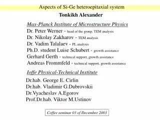
Aspects of Si-Ge heteroepitaxial system Tonkikh Alexander Max-Planck Institute of Microstructure Physics Dr. Peter Werner - head of the group, TEM analysis Dr. Nikolay Zakharov - TEM analysis Dr. Vadim Talalaev - PL analysis Ph.D. student Luise Schubert - growth assistance Gerhard Gerth - technical support, growth assistance Andreas Frommfeld - technical support, growth assistance Ioffe Physical-Technical Institute Dr.hab. George E. Cirlin Dr.hab. Vladimir G.Dubrovskii Dr.Vyacheslav A.Egorov Prof.Dr.hab. Viktor M.Ustinov Coffee seminar 03 of December 2003
Outlook Ioffe Institute presentation Brief introduction into Si-Ge MBE technique Ge islands on a Si (100) surface Kinetics of the islands formation Abnormal Sb impact Si-Ge multilayer structure Band structure Multilayer structure properties Au impact Conclusion
Scientific adviser: Nobel-prize winner Zhores I. Alferov* *Double heterostructure laser inventor Ioffe Physical-Technical Institute 194021 Politechnicheskaya 26, Saint-Petersburg, Russia http://www.ioffe.rssi.ru Founded in 1918 by Abram Fedorovich Ioffe. Ioffe-effect hole conductivity conception The main old building during winter time. The most famous scientists: Ya.I.Frenkel Exc. Pred., Kinet. of Liq. N.N.Semenov Chain chemical reactions P.L.Kapitsa super fluidity effect L.D.Landau Q.theory of el. diamagn. I.V.Kurchatov Sc. Adv. of NWP
Institute departments Center of Nanoheterostructure Physics Division of Solid State Electronics Division of Solid State Physics Division of Plasma Physics, Atomic Physics and Astrophysics Division of Physics of Dielectric and Semiconductors Educational Center Physics of Semiconductor Heterostructures Laboratory Head: Zh.I. Alferov http://www.ioffe.rssi.ru/sem_tech/ Deputy Head: Nikolai N. Ledentsov Deputy Head: Victor M. Ustinov Research activities: * physics and technology (MBE, MOCVD) of silicon and III-V semiconductor heterostructures (quantum wells, quantum dots) * electron materials science and characterization * optoelectronics, nanoelectronics (low-dimensional heterostructures) * semiconductor laser diodes, photodetectors, power and high speed semiconductor devices * postgrowth processing of semiconductors devices
Silicon MBE Principle of operation Real setup Riber Siva-45 Tsub Si substrate TSi TGe Si source Ge source MBE conditions: HV/UHV P<10-6torr Tsub<Tsi and Tge in situ control P~10-9torr in situ control: RHEED, QMS
Si-Ge heteroepitaxial system Metastable epitaxial layer against islanding and misfit dislocation formation Ge bulk Ge epilayer Island formation y x Si bulk (substrate) Si substrate Stranski-Krastanow growth mode Both diamond (face-centered cubic) like structure dGe < 4ML axGe=aSi Ge islands on a Ge wetting layer aSi=5.431Å ayGe>aGe aGe=5.658Å Δ= 2(aGe- aSi)/(aGe + aSi)x100%=4%
Start(p=0) P1(p=40) P0(p=60-80) P2(p=110) Finish(p=198) In situ observation of the island formation Reflection High Energy Electron Diffraction system (RHEED) Surface with Ge islands Ee~30KeV, λe = h/(2meEee) ~ 0.1Å ~ 1-4° dGe=7Å E-gun substrate screen The dynamic of RHEED pattern intensity on a white section Flat 2x1 reconstruction of Si(100) surface 2D-3D transition at 6.8Å (=4.8ML) of Ge! dGe=0Å
Ex situ observation of the Ge on Si islands Bimodal island shape distribution Atomic force microscopy (tapping mode) 5.5Å Ge AFM huts <105> huts+domes domes RHEED N=3.1x108cm-2 Tsub=500°C Tsub=550°C Tsub=600°C 8.5Å Ge Phase diagram for Ge islands on Si (100) surface AFM RHEED N=3.3x1010cm-2
Kinetics of Ge islands formation* Free energy of coherent island formation: Ge island Ge WL h Si L The main growth mechanism is the diffusion of the atoms from the wetting layer to the islands with D(T). The parameters of the system after the relaxation stage: Equation of material balance: g(,t) - island size distribution g(,0)=0, i=2/3 -new variable V(t) - growth rate * V.G.Dubrovskii, G.E.Cirlin and V.M.Ustinov Phys.Rev.B 68 075409 (2003)
The comparison between theory and experiment for Ge on Si(100) “hut” islands MBE parameters of the system were: h=0.9nm, V=0.0345ML/s A.A.Tonkikh et. al. Phys.Stat.Sol.(b) 236 No.1 R1 2003
Tsub=550°C, fast GR w/o Sb with Sb Sb impact on the growth of Ge islands Tsub=600°C, fast GR w/o Sb with Sb Tsub=550°C, slow GR w/o Sb with Sb
Band-edges alignment of Si-Ge heterostructures Band alignment for 1 Ge layer * Band alignment for multilayer Si-Ge ** *N.V.Vostokov et.al. Phys.Sol.St. 2004 v.46(1) p.63 **O.G.Schmidt et.al. Phys.Rev.B. 2000 v.62(24) p.16715 e- CB CB Ge Ge e- e- Ge Ge e- Si Si e- e- Si Si hh+ E VB hh+ hh+ hh+ hh+ Si Si Si Ge hh+ z II-type of band-edge alignment II-type of band-edge alignment Indirect optical transition (in real space and k-space) with aid of TO phonon Possibility to create a miniband in the conduction/valence band. ? - parameters of the structure
Properties of highly strained Si/Ge superlattice TEM plan view and cross-section Low temperature PL spectra Room temperature PL spectra Room temperature EL spectra There are still two open questions: 1) Absolute EL intensity? 2) Time resolved measurements?
Au impact on the properties of the multilayer structure SIMS Au~1016cm-3 Huge mass (atomic radius) I-group element (deep acceptor) point defects and misfit dislocations nonradiative recombination center Is it possible to avoid the misfit dislocations?
Conclusion Good corellation between experimental and theoretical data was demonstraited for the size and density distribution in ansamble of Ge island on a Si(100) surface. ! ! Unexpected Ge island array morphology was observed for surfactant (Sb) mediated growth. ! Strong room temperature electroluminescence from Si/Ge multilayer structure was demonstrated. Future tasks: To give the explanation of unexpected Sb influence on the Ge island array morphology. The optimization of the multilayer structure MBE parameters in order to get higher luminescence. Time-resolved measurements. Absolute EL intensity measurements with mesa-structure LED.
Gold wire Gold ring Contact place Cap Si n+ Si p+ (former substrate) Active zone (light emitting) Al bottom contact Plan-view image of the Si LED mesa-structure Cross-section scheme