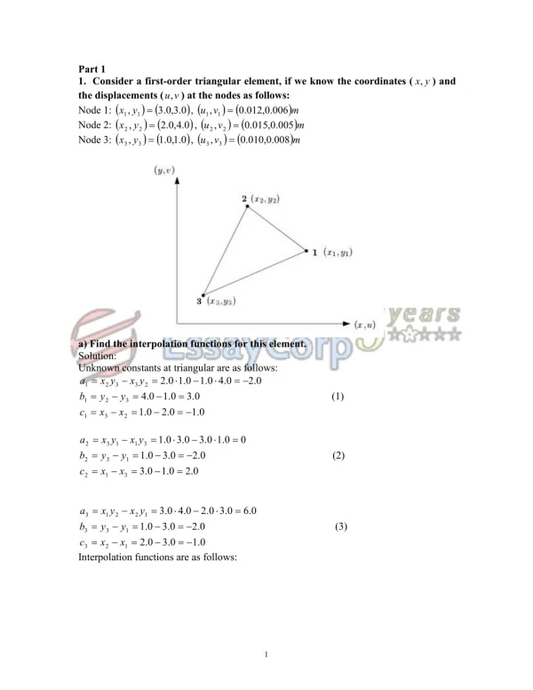
Download
1 / 20
220 likes | 647 Vues
Thermally Induced Stress in a Glass-Silicon Bonded MEMS Micro-Structure A Finite Element Analysis ( FEA ) using flexPDE. Craig E. Nelson - Consultant Engineer. The purpose of this numerical experiment is to learn about the field distribution of stress and strain in a MEMS microstructure.

E N D
Thermally Induced Stress in a Glass-Silicon Bonded MEMS Micro-Structure A Finite Element Analysis ( FEA ) using flexPDE Craig E. Nelson - Consultant Engineer
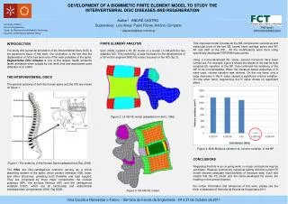
The purpose of this numerical experiment is to learn about the field distribution of stress and strain in a MEMS microstructure. This knowledge helps the engineer to better understand the stress on a bond line as will occur when anodic bonding of glass and silicon is attempted. In this model, a high bonding temperature is impressed on all parts which subsequently cool to room temperature. As the material cools, it shrinks differing amounts in different materials and in different places within a given material, thus “freezing in” stress that, unless relieved, will exist for the life of the bonded part. Depending on circumstances, the bond line may be sufficiently stressed to fail during the cooling process.
Silicon Wafer Anodic Bond Line Glass Silicon Wafer Anodic Bond Line Model Geometry
Shrinkage Shrinkage Strained Structure – Shrinkage is Greatly Magnified
Summary and Conclusions A finite element model has been developed that allows insight into the field distribution of stress and strain in an anodic bonded glass-silicon MEMS microstructure. This knowledge helps the engineer to better understand the stress and strain on the glass-silicon bond line and other parts of the solution domain. The model could be further developed in many further ways.