Download
1 / 21
210 likes | 357 Vues
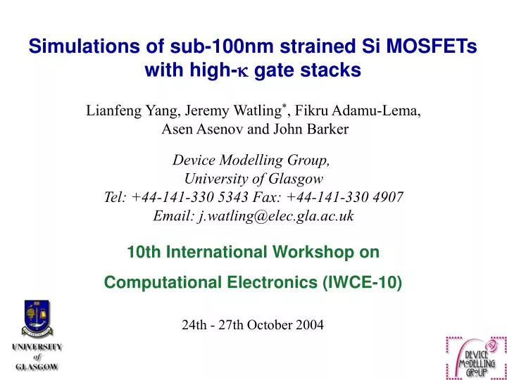
Simulations of sub-100nm strained Si MOSFETs with high- gate stacks. Lianfeng Yang , Jeremy Watling * , Fikru Adamu-Lema , Asen Asenov and John Barker Device Modelling Group, University of Glasgow Tel: +44-141-330 5343 Fax: +44-141-330 4907 Email: j.watling@elec.gla.ac.uk.

E N D
Simulations of sub-100nm strained Si MOSFETs with high- gate stacks Lianfeng Yang, Jeremy Watling*, Fikru Adamu-Lema, Asen Asenov and John Barker Device Modelling Group, University of Glasgow Tel: +44-141-330 5343 Fax: +44-141-330 4907 Email: j.watling@elec.gla.ac.uk 10th International Workshop on Computational Electronics (IWCE-10) 24th - 27th October 2004
Outline • Introduction • Device structure • (Conventional and strained Si n-MOSFETs) • Device Calibration • High- dielectrics • Results and discussion • Conclusions
Introduction • High- dielectrics • Scaling of MOSFETs beyond the 45nm technology node expected by 2010 (ITRS), requires extremely thin SiO2 gate oxides (~0.7nm) resulting in intolerably high gate leakage. • Maximise gate capacitance: • The leading contenders at present are HfO2 and Al2O3. However, there is a fundamental drawback due to the resulting mobility degradation. • Strained Si • Has already demonstrated significant enhancement for CMOS applications.
Gate Leakage current density due to gate tunnelling From ITRS 2003 edition
Mobility enhancement in strained Si Our ensemble Monte Carlo simulator includes all relevant scattering mechanisms: optical intervalley phonon, inelastic acoustic phonon, ionized impurity, along with interface roughness scattering. The simulator has been thoroughly calibrated for bulk Si transport. Monte-Carlo calculation of the low-field in- and out-of-plane electron mobilities in strained Si as a function of Ge content within the SiGe buffer; inset shows the in and out-of-plane directions.
Strained Si with high- dielectrics • IBM demonstrated the high performance of strained silicon (30% enhancement) with low leakage of high- insulators (1000 lower leakage) for maximum performance with minimum standby power • Intel presented their high- on strained Si technology at IEDM 2003 Source: IBM (VLSI 2002)
Simulation of 67nm IBM Relaxed and Strained Si n-MOSFET • Comparison between n-type Strained Si and control Si MOSFETs: • 67nm effective channel length • Similar processing and the same doping conditions In the strained Si MOSFET: • 10nm tensile strained Si layer • Strained Si on relaxed SiGe (Ge content: 15%) K.Rim, et. al., Symposium on VLSI Technology 2001 http://www.research.ibm.com/resources/press/strainedsilicon/
Strained Si n-channel MOSFET Structure Comparison between the n-type Strained Si and control Si MOSFETs: • 67nm effective channel length • Similar processing and doping conditions • Oxide thickness, tox =2.2nm (SiO2) • For the strained Si MOSFET: • 10nm strained Si layer thickness • Strained Si on relaxed SiGe (Ge content: 15%) • SiGe n-MOSFET >35% drive current enhancement • (70% high field mobility enhancement)
Device Calibration – Drift Diffusion • Drift-diffusion (MEDICI™) device simulations • Concentration dependent, Caughy-Thomas and perpendicular field dependent mobility models • Corrected Si/SiGe heterostructure parameters: band gap and band offsets, effective mass, DoS and permittivity† Calibrated ID-VG characteristics of the 67nm n-type bulk Si and strained Si MOSFETs (experimental data from Rim VLSI’01) † L. Yang, et al, ‘Si/SiGe Heterostructure Parameters for Device Simulations’,to Semiconductor Science and Technology 19, p. 1174-1182 (2004)
Device Calibration – Monte Carlo Calibrated ID-VG characteristics for 67nm conventional Si and strained MOSFETs, comparison with experimental data of Rim. Smoother interface for strained Si/SiO2 interface. See L. Yang et al, Proceedings of the 5th European Workshop on Ultimate Integration of Silicon (ULIS04), p23-26, IMEC 2004
High- dielectrics “Ideal” high- films: thermally stable, free from electron and interface traps, leakage-free, reliable and reproducible, etc. • Scalability • Leakage Replace SiO2 Fischetti, JAP’01 Ionic polarization Electronic polarization 1/Eg Highly polarized “soft” metal-oxygen bonds which screen external fields low energy lattice oscillation (soft - phonon energy) High dielectric constant Small bandgap High- dielectrics:
Remote (SO) Phonon Scattering Coupling strength between the inversion layer electrons and the soft optical (SO) phonons (from the LO modes of insulator) Fröhlich interaction Ionic polarization Electronic polarization Static Optical (high frequency) SiO2 – small difference between and High- – large difference between and Strong SO phonon scattering degrades the inversion layer carrier mobility within the MOSFET with high- gate stacks.
Monte Carlo simulations of Si MOSFET with HfO2 ID-VG characteristics of 67nm n-type Si MOSFET, with and without soft-optical phonon scattering from the HfO2 oxide.
Monte Carlo simulations of strained Si MOSFET with HfO2 ID-VG characteristics of 67nm n-type strained Si MOSFET with and without soft-optical phonon scattering from the HfO2 oxide.
Observations • We observe that those simulations which include soft-optical phonon scattering exhibit a similar percentage reduction for both Si and strained Si n-MOSFETs at the same gate over drive VG-VT = 1.0V. • The degradation in the drive current is ~40-50% at VD=0.1V and ~25% at VD=1.2V. • SO phonon scattering decreases at high-drain voltages as the ‘Fröhlich’ interaction decreases with energy.
Velocity profile along the channel Average channel velocities for the 67nm n-type bulk and strained Si MOSFETs, with and without soft-optical phonon scattering from the HfO2 gate stack.
Monte Carlo simulations of Si MOSFET, with Al2O3 ID-VG characteristics of 67nm n-type Si MOSFET, with and without soft-optical phonon scattering, from the Al2O3 oxide.
Impact of high-k on Strained Si Source: Intel, IEDM 2003
Conclusions • We have investigated the impact on the performance degradation in sub 100nm n-MOSFETs due to soft-optical phonon scattering in the presence of high- dielectrics HfO2 and Al2O3. • A device current degradation of around 25% at VG-VT=1.0V and VD=1.2V is observed for conventional and strained Si devices with a 2.2nm EOT HfO2. Correspondingly a current degradation of around 10% is observed for conventional and strained Si devices with a 2.2nm EOT Al2O3. • Our results indicate that the performance degradation associated with high- gate stack MOSFETs can be compensated by the introduction of strained Si channels. • The infancy of high- gate fabrication techniques means that overall performance degradation associated with high- gate dielectrics is expected to be worse than the predictions here.