Download
1 / 1
20 likes | 115 Vues
Eindhoven MOS-AK Meeting April 4, 2008. Accurate FinFET modeling at high temperatures Cerdeira 1 , M. Estrada 1 , J. Alvarado 2 , V. Kilchytska 2 and D. Flandre 2

E N D
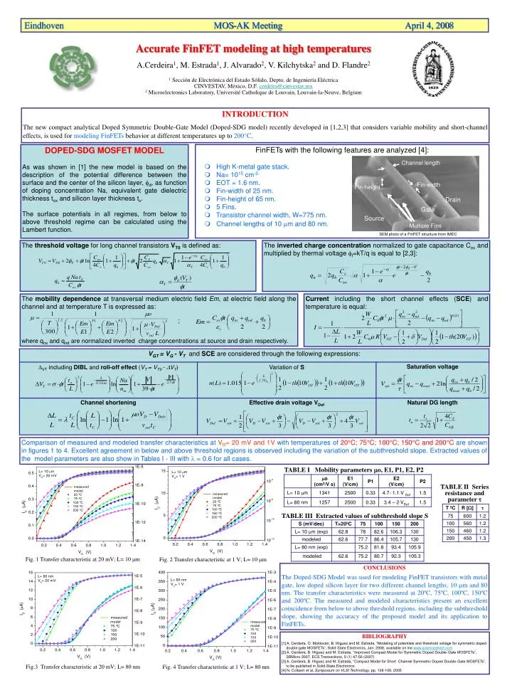
Eindhoven MOS-AK Meeting April 4, 2008 • Accurate FinFET modeling at high temperatures • Cerdeira1, M. Estrada1, J. Alvarado2, V. Kilchytska2 and D. Flandre2 • 1 Sección de Electrónica del Estado Sólido, Depto. de Ingeniería Eléctrica • CINVESTAV, México, D.F. cerdeira@cinvestav.mx • 2Microelectronics Laboratory, Université Catholique de Louvain, Louvain-la-Neuve, Belgium INTRODUCTION The new compact analytical Doped Symmetric Double-Gate Model (Doped-SDG model) recently developed in [1,2,3] that considers variable mobility and short-channel effects, is used for modeling FinFETs behavior at different temperatures up to 200°C. DOPED-SDG MOSFET MODEL As was shown in [1] the new model is based on the description of the potential difference between the surface and the center of the silicon layer, d, as function of doping concentration Na, equivalent gate dielectric thickness tox and silicon layer thickness ts. The surface potentials in all regimes, from below to above threshold regime can be calculated using the Lambert function. • FinFETs with the following features are analyzed [4]: • High K-metal gate stack. • Na= 1015 cm-3. • EOT = 1.6 nm. • Fin-width of 25 nm. • Fin-height of 65 nm. • 5 Fins. • Transistor channel width, W=775 nm. • Channel lengths of 10 m and 80 nm. SEM photo of a FinFET structure from IMEC Channel length Fin-width Fin-height Drain Gate Source Multiple Fins The threshold voltage for long channel transistors VT0 is defined as: The invertedcharge concentration normalized to gate capacitance Cox and multiplied by thermal voltage t=kT/q is equal to [2,3]: The mobility dependence at transversal medium electric field Em, at electric field along the channel and at temperature T is expressed as: ; where qns and qnd are normalized inverted charge concentrations at source and drain respectively. Current including the short channel effects (SCE) and temperature is equal: Comparison of measured and modeled transfer characteristics atVD= 20 mV and 1Vwith temperatures of20°C; 75°C; 100°C; 150°C and 200°Care shown in figures 1 to 4. Excellent agreement in below and above threshold regions is observed including the variation of the subthreshold slope. Extracted values of the model parameters are also show in Tables I - III with = 0.6 for all cases. TABLE I Mobility parameters o, E1, P1, E2, P2 TABLE II Series resistance and parameter TABLE III Extracted values of subthreshold slope S Fig. 1 Transfer characteristic at 20 mV; L= 10 m Fig. 2 Transfer characteristic at 1 V; L= 10 m CONCLUSIONS The Doped-SDG Model was used for modeling FinFET transistors with metal gate, low doped silicon layer for two different channel lengths, 10 m and 80 nm. The transfer characteristics were measured at 20ºC, 75ºC, 100ºC, 150ºC and 200ºC. The measured and modeled characteristics present an excellent coincidence from below to above threshold regions, including the subthreshold slope, showing the accuracy of the proposed model and its application to FinFETs. BIBLIOGRAPHY [1] A. Cerdeira, O. Moldovan, B. Iñiguez and M. Estrada, “Modeling of potentials and threshold voltage for symmetric doped double-gate MOSFETs”, Solid-State Electronics, Jan. 2008, available on ine www.sciencedirect.com [2] A. Cerdeira, B. Iñiguez and M. Estrada, “Improved Compact Model for Symmetric Doped Double-Gate MOSFETs”, SBMicro 2007, ECS Transactions, 9 (1) 47-56 (2007) [3] A. Cerdeira, B. Iñiguez and M. Estrada, “Compact Model for Short Channel Symmetric Doped Double-Gate MOSFETs”, to be published in Solid-State Electronics [4] N. Collaert et al.,Symposium on VLSI Technology, pp. 108-109, 2005 Fig.3 Transfer characteristic at 20 mV; L= 80 nm Fig. 4 Transfer characteristic at 1 V; L= 80 nm