Download
1 / 30
300 likes | 401 Vues
Elimination or Significant Reduction of the Effects of Stress Concentrators by Nanosizing. Collaborators: P. Deymier, MSE, Univ. of Arizona E. Enikov, AME, Univ. of Arizona C. Haynie, CEEM, Univ. of Arizona. Central Theme: When spatial dimensions are below a material

E N D
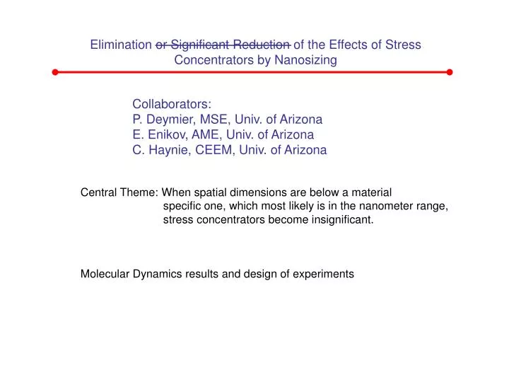
Elimination or Significant Reduction of the Effects of Stress Concentrators by Nanosizing Collaborators: P. Deymier, MSE, Univ. of Arizona E. Enikov, AME, Univ. of Arizona C. Haynie, CEEM, Univ. of Arizona Central Theme: When spatial dimensions are below a material specific one, which most likely is in the nanometer range, stress concentrators become insignificant. Molecular Dynamics results and design of experiments
Components with Nanodimensional Structure Technologies presently exist, and are becoming more efficient, in producing components of nanodimenions (nanolaminates, nanoflakes, nanofibers, comb, etc.) Nano-composite for energetic pigment applications. Courtesy: Sigma Tech. Intl., Inc. 10,000 layers of alternating metal/polymer. Each layer is 20-30nm thick. Courtesy: Sigma Tech. Intl., Inc.
Future Technologies One Potential Important Future application: Hydrogen storage by adsorption, where intentional surfaces, pores … (STRESS CONCENTRATORS) increase the surface area. The mechanical integrity is paramount, and insensitivity to defects is a reliability design dream come true – stress concentrators are ubiquitous
Nature Knows Courtesy: Gao et al, 2003, Proc. Nat. Acad. Sci. The basic building components in many biological materials remarkable for their properties are at the nanoscale (mineral/organic). Why the Nanoscale ??
Stress Concentrators Nano stress concentrators (NSCs) here indicate defects such as impurities, inclusions, cracks, pores; defects other than NSCs, e.g. dislocations, are also addressed yet they are considered part of the “bulk” material Examples: from roughness of substrate, impurities, pores, inclusions In biological materials NSCs are trapped proteins within mineral crystals during biomineralization. Consistency in these materials is remarkable.
Size Effects – Since Galileo Galilei and Leonardo da Vinci Note on Hall-Petch effects Considering for a brittle material: g=1J/m2, E=100GPa, sth=E/30] and a=p1/2 we obtain hcr = 30nm
Size Effects: Well Studied Yield strengthof electroplated Cu thin films as a function of film thickness t. In the plot of these nanoindentation experimental results, sizing to ~200nm, the yield stress was assumed as the 1/3 of the hardness. Courtesy of Volinsky and Gerberich, 2003, Microel. Engr. Journal. Insensitivity to NSCs has not been speculated, Plus difficulties in studying (experimental and simulation) Koehler, 1970: a structure comprised of alternating layers of two suitable metals exhibits a resistance to plastic deformation that would be greater than that expected from a homogenous alloy of the two.
Below Certain Nanoscales: More than Size Effects Expected Behavior – Insensitivity to Defects For NSC diameter = ½ thickness hcr
3D views Side views stress (Pa) strain MD Simulations (EAM) – Cu Crystal with a NSC Pulled in (001) Over 2,000,000 atoms Many slip planes High strain rate Non periodic BC
3D views side views Stress (Pa) strain MD Simulations (EAM) – Cu Crystal w/o NSC Pulled in (001) (111) slip planes form Over 2,000,000 atoms Two slip planes High strain rate Non Periodic BC
small system with NSC large system, no NSC (b) (a) stress (Pa) large system with same NSC stress (Pa) small system, no NSC strain strain Insensitivity to the NSCs Large system: 28.88x28.88x28.88 nm3 (over 2,000,000 atoms) 3.0x3.0x0.4 nm3 NSC Small system: 18.05x18.05x18.05 nm3 (~ 500,000 atoms) 3.0x3.0x0.4 nm3 NSC
N with NSC without NSC strain Why the Insensitivity ? If, on average, the energy required for forming each atomistic defect is constant, this explains insensitivity of the material to NSCs Total number of atomistic defects, N, versus strain for the small Cu(001) system with and without NSC. Plot was obtained from atom positions at five strain levels during deformation. Role of Surfaces: ratio surface/volume ~ 1/a important for small a
Surfaces – large system, high strain rate, non periodic BC With NSC Without NSC External surfaces start dominating as atomistic defect initiation sites
Surfaces, small system, high strain rate, non periodic BC With NSC Without NSC External surfaces start dominating as atomistic defect initiation sites
Surfaces, small system, high strain rate, periodic BC With NSC, side views Without NSC, side views Loaded surfaces start dominating as atomistic defect initiation sites for two large (infinite) lateral dimensions (periodic BC). NSCs stimulate the clustering of atomistic defects.
Slower Strain Rates – Non Periodic BC With NSC N N Without NSC With NSC Without NSC Strain Strain Large System Small System Number of Atomistic Defects Versus Strain, (one realization, even though process is statistical)
Slower Strain Rates – Non Periodic BC Stress (Pa) Strain Slow strain rate, large system, no NSC and 2 NSC sizes (3 curves) Stress (Pa) Strain Slow strain rate, small system, no NSC and 1 large NSC
Surprise: Slower Strain Rates – Periodic BC Without NSC Without NSC N N With NSC With NSC Strain Strain Large System Small System Number of Atomistic Defects Versus Strain. NSCs stimulate the clustering of atomistic defects.
Slower Strain Rates – Periodic BC Without NSC Stress (Pa) With NSC 1 With NSC 2 Strain Slow strain rate, large system, no NSC and 2 NSC sizes (3 curves) Without NSC Stress (Pa) With NSC Strain Slow strain rate, small system, no NSC and 1 NSC
Slower strain rate, non periodic BC Large system with NSC Large system, no NSC
Slower strain rate, non periodic BC – side views Large system with NSC Large system, no NSC
Slower strain rate, periodic BC Large system with NSC Large system, no NSC Atomistic defects cluster at the loading surfaces
Slower strain rate, periodic BC – side views Large system with NSC Large system, no NSC Atomistic Defects cluster at the loading surfaces
Experiments Nanoindentation: not appropriate for this work The very local indenter, which introduces a NSC, interacts strongly with pre-existing NSCs; two samples (films of different thickness) are unlikely to have the same NSCs positioned near the indenter in a similar fashion.
(Left) SPM 2.5x2.5 μm2 image of metal nanotubes, (right) higher magnification SPM image. The diameter of the metal tubes is about 40nm and the thickness about 10nm. Experiments
(b) (a) Deflection (load) Probe’s Vertical Position (displacement) (c) The SPM probe is pushed on the metal tubes lying on a flat wafer. Height image using contact mode (low resolution) after load is imposed by Force Volume SPM. (a) 1x1μm, (b) 500x500nm; the marked area (red ellipse) was damaged during the Force Volume SPM. (c) Typical force displacement curve. Limitations …. force volume SPM.
Experiments Membrane tests Smooth Probe
Schematic of the membrane problem. Nine MD cells are coupled to FEs discretizing the rest of the film. The handshake region coupling the MD and FE regions is wavelet-based, filtering high frequencies that create unrealistic reflections at the interface. Simulation of Experiments
Simulation Issues • The MD-FE interface (not resolved – dispersion issues) • use a wavelet-based absorbing interphase • Propagation of atomistic defects in the FE domain • use kMC (kinetic Monte Carlo) as intermediate technique • to avoid artificial dislocation pileup • Has been tested (Frantziskonis & Deymier, 2000)
Conclusions For Cu subjected to tensile strain, the critical dimensions for the effects of NSCs are larger than the examined (up to) 28.8nm. Multiscale simulations are necessary to identify critical dimensions and also examine slower strain rates. The spatial pattern of atomistic defects that develops during straining is different for a system with NSCs than one without NSCs.Yet, the number of atomistic defects (number of atoms with modified coordination number) seems to be independent of the NSCs. Samples larger than critical tend to cluster atomistic defects. Surfaces are instrumental in initiating atomistic defects. Surface Effects, also instrumental at macro-scales, are beneficial at nano-scales, i.e. they eliminate the effects of stress concentrators. Strain rate (1 order of magnitude difference) does not alter the conclusions Computer power and experimental difficulties of the past did not allow one to even speculate that such a (materials processing and reliability) dream may be true!