Download
1 / 1
10 likes | 122 Vues
Planar Antenna-Coupled Hot-electron Microbolometer. Shafinaz Ali 1 , Dan Mccammon 1 , Lance D. Cooley 2 , Kari.L.Nelms 1 , John Peck 3 , Daniel Prober 4 , Dan Swetz 1 , Peter Timbie 1 , Daniel van der Weide 3

E N D
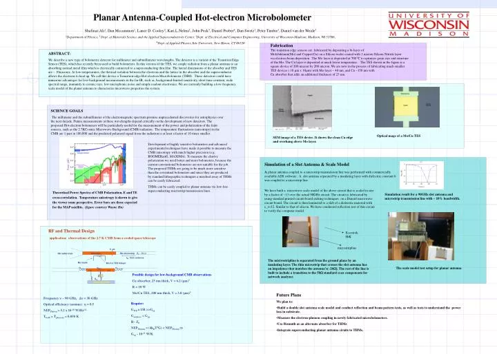
Planar Antenna-Coupled Hot-electron Microbolometer Shafinaz Ali1, Dan Mccammon1, Lance D. Cooley2, Kari.L.Nelms1, John Peck3, Daniel Prober4, Dan Swetz1, Peter Timbie1, Daniel van der Weide3 1Department of Physics, 2 Dept. of Materials Science and the Applied Superconductivity Center, 3Dept. of Electrical and Computer Engineering, University of Wisconsin-Madison, Madison, WI 53706, 4Dept. of Applied Physics,Yale University, New Haven, CT 06520 Fabrication The transition edge sensors are fabricated by depositing a bi-layer of Molybdenum(Mo) and Copper(Cu) on a Silicon wafer coated with 1 micron Silicon Nitride layer via electron beam deposition. The Mo layer is deposited at 700 0C to optimize grain size and structure of the Mo. The Cu layer is deposited at much lower temperature. The TES shown in the figure is a square device of 200 micron by 200 micron. We are now in the process of fabricating much smaller TES devices ( 10 mm x 10mm) with Mo layer ~ 40 nm, and Cu ~150 nm with Cu absorber that adds an additional thickness of 23 nm. ABSTRACT: We describe a new type of bolometric detector for millimeter and submillimeter wavelengths. The detector is a variant of the Transition Edge Sensor (TES), which has recently been used to build bolometers. In this version of the TES, we couple radiation from a planar antenna to an absorbing normal metal film which is electrically connected to a superconducting thin film. The lateral dimensions of the absorber and TES are ~ 10microns. At low temperatures, the thermal isolation between the electrons and the lattice in the absorber and the superconductor allows the electrons to heat up. We call this device a Transition-edge Hot-electron Microbolometer (THM). These detectors could have numerous advantages for low-background measurements in the far-IR, such as, background-limited sensitivity, short time constant, wide spectral range, immunity to cosmic rays, low microphonic noise and simple readout electronics. We are currently building a low-frequency scale model of the planar antenna to characterize microwave properties the system. SCIENCE GOALS The millimeter and the submillimeter of the electromagnetic spectrum promise unprecedented discoveries for astrophysics over the next decade. Future measurements at these wavelengths depend critically on the development of new detectors. The proposed Hot-electron bolometers will be particularly useful for the measurement of the power and polarization of the faint sources, such as the 2.7KCosmic Microwave Background (CMB) radiation. The temperature fluctuations (anisotropy) in the CMB are 1 part in 100,000 and the predicted polarized signal from the radiation is at least a factor of 10 times smaller. Optical mage of a Mo/Cu TES SEM image of a TES device. It shows the clean Cu edge and overhang above Mo layer. Development of highly sensitive bolometers and advanced experimental techniques have made it possible to measure the CMB anisotropy with much higher precision (e.g. BOOMERanG, MAXIMA). To measure the elusive polarization we need better and more bolometers, because the current conventional bolometers are not suitable for the job. The proposed THMs are going to be much more sensitive than the coventinal bolometers and since they are produced by standard lithographic techniques a matched array of THMs can be easily fabricated. THMs can be easily coupled to planar antenna via low-loss superconducting microstrip transmission lines. Simulation of a Slot Antenna & Scale Model Aplanar antenna coupled to a microstrip transmission line was performed with commercially available ADS software. A slot antenna separated by a insulating layer with dielectric constant 6 was coupled to a microstrip line. We have built a microwave scale model of the above circuit that is scaled in size by a factor of ~13 over the actual 90GHz circuit. The circuit is fabricated by using standard printed-circuit board etching techniques on a Duroid microwave circuit board. The circuit is then laminated to a slab of a dielectric material with e_r=12. Similar to that of silicon. We have conducted reflection test of this circuit to verify the computer model. Theoretical Power Spectra of CMB Polarization, E and TE cross-correlation. Temperature anisotropy is shown to give the viewer some perspective. Error bars are those expected for the MAP satellite. (figure courtesy Wayne Hu) Simulation result for a 90GHz slot antenna and microstrip transmission line with ~ 10% bandwidth. RF and ThermalDesign Eccostok HiK application: observations of the 2.7 K CMB from a cooled space telescope microstripline 6 m Nb microstrip Z0 ~ 10 W Nb radial stub Absorber IRF from antenna The mictrostripline is separated from the ground plane by an insulating layer. The thin microstrip that crosses the slot antenna has an impedence that matches the antenna’s(~20W). The rest of the line is built to include a transition to the 50W standard coax components for network analyzer. Mo leads Mo/Cu TES bilayer The scale model test setup for planar antenna. GAndreev GAndreev GWF e’s e’s Possible design for low-background CMB observations: Cu absorber, 23 nm thick, V = 6.2 (m)3 R = 10 W Mo/Cu TES, 200 nm thick, V = 3.0 (m)3 e’s Gep Lattice phonons • Future Plans • We plan to: • Build a double slot antenna scale model and conduct reflection and beam pattern tests, as well as tests to understand the power loss in substrate. • Measure the electron-phonon coupling in newly fabricated microbolometers. • Use Bismuth as an alternate absorber for THMs • Integrate superconducting planar antenna ciruits to THMs. Frequency ~ 90 GHz, = 30 GHz Optical efficiency (assume) = 0.5 NEPPhoton= 5.2 x 10⁻¹⁸ W/Hz1/2 Tbath = Tphonons = 0.050 K Require: GWF a 1/R >>Gep Gandreev < Gep R~ Z0 NEPPhonon = (4kBT2G) < NEPPhoton Gep ~ 10-11 W/K