Download
1 / 29
290 likes | 310 Vues
Learn how to interact with peripherals using memory-mapped I/O in microcontrollers. This course covers bus architectures, assembly programming, and examples with push buttons and LED drivers.

E N D
EECS 373 Design of Microprocessor-Based Systems Prabal Dutta University of Michigan Memory-Mapped I/O Bus Architectures Slides developed in part by Mark Brehob & Prabal Dutta
Today… Memory-Mapped I/O Example Bus with Memory-Mapped I/O Bus Architectures
Course Roadmap: Beyond the CPU C Assembly Machine Code Central Processing Unit EECS 370 Software Hardware ISA bl (interrupt) ldr (read) str (write) System Buses AHB/APB Interrupts GPIO/INT Internal & External Memory Timers USART DAC/ADC Internal External EMC SPI DAC I2C ADC Input UART Output Capture Compare Interrupt
Memory-mapped I/O • Microcontrollers have many interesting peripherals • But how do you interact with them? • Need to: • Send commands • Configure device • Receive data • But we don’t want new processor instructions for everything • Actually, it would be great if the processor didn’t know anything weird was going on at all
Memory-mapped I/O • Instead of real memory, some addresses map to I/O devices instead Example: • Address 0x80000004 is a General Purpose I/O (GPIO) Pin • Writing a 1 to that address would turn it on • Writing a 0 to that address would turn it off • Reading at that address would return the value (1 or 0)
Memory-mapped I/O • Instead of real memory, some addresses map to I/O devices instead • But how do you make this happen? • MAGIC isn’t a bad guess, but not very helpful Let’s start by looking at how a memory bus works
Today… Memory-Mapped I/O Example Bus with Memory-Mapped I/O Bus Architectures
Bus terminology • Any given transaction have an “initiator” and “target” • Any device capable of being an initiator is said to be a “bus master” • In many cases there is only one bus master (single master vs. multi-master). • A device that can only be a target is said to be a slave device.
Basic example Let’s demonstrate a hypothetical example bus • Characteristics • Asynchronous (no clock) – why? • One Initiator and One Target • Signals • Addr[7:0], Data[7:0], CMD, REQ#, ACK# • CMD=0 is read, CMD=1 is write. • REQ# low means initiator is requesting something. • ACK# low means target has done its job.
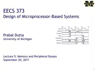
0x24 ?? ?? Read transaction Initiator wants to read location 0x24 A BC D E F G HI I: Addr[7:0] I: CMD T: Data[7:0] I: REQ# T: ACK# 0x55 ?? ?? I: Transaction is complete, Bus is idle G: Initiator sets REQ# high, Stops driving Addr and CMD H: Target sets ACK# to high, Stops driving data A: Initiator sets Addr = 0x24, CMD = 0 E: Target sets ACK# to low D: Target drives data F: Initiator sees data and latches it B: Initiator sets REQ# to low C: Target sees read request A B C D E F G H I
A read transaction • Say initiator wants to read location 0x24 • Initiator sets Addr=0x24, CMD=0 • Initiator then sets REQ# to low • Target sees read request • Target drives data onto data bus • Target then sets ACK# to low • Initiator grabs the data from the data bus • Initiator sets REQ# to high, stops driving Addr and CMD • Target stops driving data, sets ACK# to high terminating the transaction • Bus is seen to be idle
A write transaction • Say initiator wants to write 0xF4 location 0x31 • Initiator sets Addr=0x24, CMD=1, Data=0xF4 • Initiator then sets REQ# to low • Target sees write request • Target reads data from data bus (only needs to store in register, not write all the way to memory) • Target then sets ACK# to low. • Initiator sets REQ# to high, stops driving other lines • Target sets ACK# to high, terminating the transaction • Bus is seen to be idle.
Returning to memory-mapped I/O Now that we have an example bus, how would memory-mapped I/O work on it? Example peripherals 0x04: Push Button - Read-Only Pushed -> 1 Not Pushed -> 0 0x05: LED Driver - Write-Only On -> 1 Off -> 0
The push-button(if Addr=0x04 write 0 or 1 depending on button) Addr[7] Addr[6] ACK# Addr[5] Addr[4] Addr[3] Addr[2] Addr[1] Addr[0] REQ# Data[7] CMD Data[6] Data[5] Data[4] Data[3] Data[2] Data[1] Data[0] Button (0 or 1)
Delay ACK# Data[7] Data[6] Data[5] 0 Data[4] Data[3] Data[2] Data[1] Button (0 or 1) Data[0] The push-button(if Addr=0x04 write 0 or 1 depending on button) Addr[7] Addr[6] Addr[5] Addr[4] Addr[3] Addr[2] Addr[1] Addr[0] REQ# CMD What about CMD?
Addr[7] DATA[7] Addr[6] DATA[6] DATA[5] Addr[5] Addr[4] DATA[4] Addr[3] DATA[3] DATA[2] Addr[2] Addr[1] DATA[1] Addr[0] DATA[0] The LED(1 bit reg written by LSB of address 0x05) ACK# REQ# LED CMD
Addr[7] DATA[7] Addr[6] DATA[6] Addr[5] DATA[5] Delay ACK# Addr[4] DATA[4] D Addr[3] DATA[3] DATA[2] Addr[2] clock Addr[1] DATA[1] DATA[0] Addr[0] LED The LED(1 bit reg written by LSB of address 0x05) REQ# CMD
Let’s write a simple assembly program Light on if button is pressed. Peripheral Details 0x04: Push Button - Read-Only Pushed -> 1 Not Pushed -> 0 0x05: LED Driver - Write-Only On -> 1 Off -> 0
Today… Memory-Mapped I/O Example Bus with Memory-Mapped I/O Bus Architectures
Driving shared wires • It is commonly the case that some shared wires might have more than one potential device that needs to drive them. • For example there might be a shared data bus that is used by the targets and the initiator. We saw this in the simple bus. • In that case, we need a way to allow one device to control the wires while the others “stay out of the way” • Most common solutions are: • using tri-state drivers (so only one device is driving the bus at a time) • using open-collector connections (so if any device drives a 0 there is a 0 on the bus otherwise there is a 1)
Or just say no to shared wires. • Another option is to not share wires that could be driven by more than one device... • This can be really expensive. • Each target device would need its own data bus. • That’s a LOT of wires! • Not doable when connecting chips on a PCB as you are paying for each pin. • Quite doable (though not pretty) inside of a chip.
Wire count • Say you have a single-master bus with 5 other devices connected and a 32-bit data bus. • If we share the data bus using tri-state connections, each device has “only” 32-pins. • If each device that could drive data has it’s own bus… • Each slave would need _____ pins for data • The master would need ______ pins for data • Again, recall pins==$$$$$$.
Accessing memory locations from C #define SYSREG_SOFT_RST_CR 0xE0042030 uint32_t *reg = (uint32_t *)(SYSREG_SOFT_RST_CR); main () { *reg |= 0x00004000; // Reset GPIO hardware *reg &= ~(0x00004000); } Memory has an address and value Can equate a pointer to desired address Can set/get de-referenced value to change memory
What happens when this“instruction” executes? #include <stdio.h> #include <inttypes.h> #define REG_FOO 0x40000140 main () { uint32_t *reg = (uint32_t *)(REG_FOO); *reg += 3; printf(“0x%x\n”, *reg); // Prints out new value }
“*reg += 3” is turned into a ld, add, str sequence • Load instruction • A bus read operation commences • The CPU drives the address “reg” onto the address bus • The CPU indicated a read operation is in process (e.g. R/W#) • Some “handshaking” occurs • The target drives the contents of “reg” onto the data lines • The contents of “reg” is loaded into a CPU register (e.g. r0) • Add instruction • An immediate add (e.g. add r0, #3) adds three to this value • Store instruction • A bus write operation commences • The CPU drives the address “reg” onto the address bus • The CPU indicated a write operation is in process (e.g. R/W#) • Some “handshaking” occurs • The CPU drives the contents of “r0” onto the data lines • The target stores the data value into address “reg”
Details of the bus “handshaking” dependon the particular memory/peripherals involved • SoC memory/peripherals • AMBA AHB/APB • NAND Flash • Open NAND Flash Interface (ONFI) • DDR SDRAM • JEDEC JESD79, JESD79-2F, etc.
Why use a standardized bus? • Downsides • Have to follow the specification • Probably has actions that are unnecessary • Upside • Generic systems • Allows modules to be reused on different systems
Questions? Comments? Discussion?