Download
1 / 25
380 likes | 1k Vues
Magnetoresistive Random Access Memory (MRAM). Menelaos – Charalampos Tsigkourakos Christos Trompoukis. Outline. Introduction Magnetic Core RAM Magnetoresistance Giant Magnetoresistance (GMR) Tunnel Magnetoresistance (TMR) Spin Valve MRAM Fixed Layer Reading Process Writing Process

E N D
Magnetoresistive Random Access Memory (MRAM) Menelaos – Charalampos Tsigkourakos Christos Trompoukis
Outline • Introduction • Magnetic Core RAM • Magnetoresistance • Giant Magnetoresistance (GMR) • Tunnel Magnetoresistance (TMR) • Spin Valve • MRAM • Fixed Layer • Reading Process • Writing Process • Characteristics • Other RAM Technologies • MRAM Vs Other RAM Technologies • Future MRAM Improvements • MRAM Status
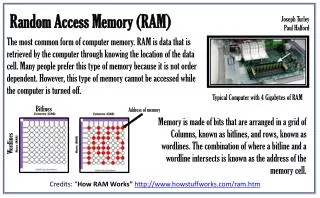
Introduction • Why can’t your pc simply turn on like your television? • MRAM uses magnetism rather than electrical power to store bits of data. • No refresh is needed to retain the data. • For users of laptops and other mobile devices, suchas MP3 players and cell phones, MRAM is the holy grail of longer battery life.
Magnetic Core RAM By the early 1960’s, Magnetic Core RAM became largely universal as main memory, replacing drum memory
Magnetic Core RAM The memory cellsconsist of wiredthreaded tiny ferrite rings (cores). X and Y lines to apply the magnetic filed. Sense/Inhibit line to ‘read’ the current pulse when the polarization of the magnetic field changes.
Giant Magnetoresistance (GMR) Two thin films of alteringferromagnetic materials and a non-magnetic layer-spacer. 10-80% decrease in electrical resistance
Tunnel Magnetoresistance (TMR) Two thin films of alteringferromagnetic materials and an insulating spacer. Fe/MgO/Fe junctions reach over 200%decrease in electrical resistance at room temperature 600 (room temperature)-1100 (4.2 K) % TMR at junctions of CoFeB/MgO/CoFeB
Tunnel Magnetoresistance (TMR) In ferromagnetic metals electronic bands are exchange split which implies different densities of states at the Fermi energy for the up- and down-spin electrons.
Tunnel Magnetoresistance (TMR) Spin of electrons is conserved in the tunneling process. Tunneling of up- and down-spin electrons are two independent processes → conductance occurs in the two independent spin channels. Electrons originating from one spin state of the first ferromagnetic film are accepted by unfilled states of the same spin of the second film.
Spin Valve GMR Hard layer: magnetization is fixed. Soft layer: magnetization is free to rotate. Thin non-ferromagnetic spacer ~3 nm. Spacer materialCu (copper) andferromagnetic layers NiFe (permalloy). This configuration used in hard drives.
Magnetic Tunnel Junction (MTJ) Commonly used insulating materials are Aluminum oxide (Al2O3) and crystalline Magnesium oxide (MgO)
MRAM One of the two plates is a permanent magnet set to a particular polarity, the other's field will change to match that of an external field.
MRAM: Fixed layer The bottom layers give an effect of fixed (pinned) layer dueto interlayer exchange coupling between ferromagnetic and spacer layer of synthetic antiferromagnetic.
MRAM: Reading process Transistor is “ON” Measuring of electrical resistance of a small sense current from a supply line through the cell to the ground.
MRAM: Writing process Transistor is “OFF” When current is passed through the write lines, an induced magnetic field is created at the junction, which alters the polarity of the free layer.
MRAM: Writing process In order to change the polarity of the free layer, both fields are necessary. Only the bit inwhich current is applied in both hard and easy axis will be written.The other bits will remain half-select.
MRAM: Characteristics • Non-volatility • Infinite endurance • High speed performance • Low cost
Other RAM Technologies DRAM Each bit of data is stored in a separate capacitor within an integrated circuit Characteristics • Volatile • The highest density RAM currently available • The least expensive one • Moderately fast
Other RAM Technologies SRAM Each bit is stored on four transistors that form two cross-coupled inverters Characteristics • Expensive • Volatile • Fast • Low power consumption • Less dense than DRAM
Other RAM Technologies Flash RAM Stores information in an array of memory cells made from floating-gate transistors Characteristics • Cheap • Non-volatile • Slow • Enormously durable • Limited endurance
MRAM Vs Other RAM Technologies MRAM combines the best characteristics of DRAM, SRAM and Flash RAM
Future MRAM Improvements Thermal Assisted Switching • Solves the first-generation selectivity and stability problems • Cost-effective and scalable memory technology to at least the 32nm node
Future MRAM Improvements Spin Torque Transfer • No applied magnetic field • Utilizes heavily spin polarized current • The magnetization of nano-elements is flipped back and forth • Still has challenges in basic physics and materials to overcome
MRAM Status • 2003 - A 128 kbit MRAM chip was introduced, manufactured with a 180 nm lithographic process • 2004 - Infineon unveiled a 16-Mbit prototype, manufactured with a 180 nm lithographic process • 2005 - Sony announced the first lab-produced spin-torque-transfer MRAM • 2007 - Tohoku University and Hitachi developed a prototype 2 Mbit Non-Volatile RAM Chip employing spin-transfer torque switching • 2008 - Scientists in Germany have developed next-generation MRAM that is said to operate with write cycles under 1 ns. • 2009 - Hitachi and Tohoku University demonstrated a 32-Mbit spin-transfer torque RAM (SPRAM)