Download
1 / 35
360 likes | 531 Vues
CS61C : Machine Structures Lecture 5.2.1 CPU Design III: Control 2004-07-21 Kurt Meinz inst.eecs.berkeley.edu/~cs61c. Inst Memory. Adr. Adder. Mux. Adder. Putting it All Together:A Single Cycle Datapath. Instruction<31:0>. <0:15>. <21:25>. <16:20>. <11:15>. Rs. Rt. Rd. Imm16.

E N D
CS61C : Machine StructuresLecture 5.2.1CPU Design III: Control2004-07-21Kurt Meinzinst.eecs.berkeley.edu/~cs61c
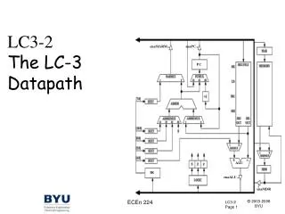
Inst Memory Adr Adder Mux Adder Putting it All Together:A Single Cycle Datapath Instruction<31:0> <0:15> <21:25> <16:20> <11:15> Rs Rt Rd Imm16 RegDst nPC_sel ALUctr MemWr MemtoReg Equal Rt Rd 0 1 Rs Rt 1 RegWr 5 5 5 busA Rw Ra Rb = 00 busW 32 32 32-bit Registers ALU 0 32 busB 32 0 PC 32 Mux Mux Clk 32 WrEn Adr 1 1 Data In Data Memory imm16 Extender 32 PC Ext Clk 16 imm16 Clk ExtOp ALUSrc
. . . . . . . . . . . . Recall: Clocking Methodology Clk • All storage elements are clocked by the same clock edge • Cycle Time = CLK-to-Q + Longest Delay Path + Setup + Clock Skew Setup Hold Setup Hold Don’t Care
. . . . . . . . . . . . Clocking Methodology Clk • Storage elements clocked by same edge • Being physical devices, flip-flops (FF) and combinational logic have some delays • Gates: delay from input change to output change • Signals at FF D input must be stable before active clock edge to allow signal to travel within the FF, and we have the usual clock-to-Q delay • “Critical path” (longest path through logic) determines length of clock period
PC ALU Clk An Abstract View of the Critical Path Critical Path (Load Operation) = Delay clock through PC (FFs) + Instruction Memory’s Access Time + Register File’s Access Time + ALU to Perform a 32-bit Add + Data Memory Access Time + Stable Time for Register File Write • This affects how much you can overclock your PC! Ideal Instruction Memory Instruction Rd Rs Rt Imm 5 5 5 16 Instruction Address A Data Address 32 Rw Ra Rb 32 Ideal Data Memory 32 32 32-bit Registers Next Address Data In B Clk Clk 32
How to Design a Processor: step-by-step • 1. Analyze instruction set architecture (ISA) => datapath requirements • meaning of each instruction is given by the register transfers • datapath must include storage element for ISA registers • datapath must support each register transfer • 2. Select set of datapath components and establish clocking methodology • 3. Assemble datapath meeting requirements • 4. Analyze implementation of each instruction to determine setting of control points that effects the register transfer. • 5. Assemble the control logic (hard part!)
A Single Cycle Datapath • Rs, Rt, Rd, Imed16 connected to datapath • We have everything except control signals Instruction<31:0> nPC_sel Instruction Fetch Unit Rd Rt <0:15> <21:25> <16:20> <11:15> Clk RegDst 1 0 Mux Rt Rs Rd Imm16 Rs Rt RegWr ALUctr Zero 5 5 5 MemWr MemtoReg busA Rw Ra Rb busW 32 32 32-bit Registers 0 ALU 32 busB 32 0 Clk 32 Mux Mux 32 1 WrEn Adr 1 Data In 32 Data Memory imm16 Extender 32 16 Clk ALUSrc ExtOp
nPC_MUX_sel Inst Memory Adr 1 Adder 00 Mux PC Adder Clk imm16 PC Ext Meaning of the Control Signals: IF • nPC_MUX_sel: 0 PC <– PC + 4 1 PC <– PC + 4 + {SignExt(Im16) , 00 } “n”=next
Meaning of the Control Signals • MemWr: 1 write memory • MemtoReg: 0 ALU; 1 Mem • RegDst: 0 “rt”; 1 “rd” • RegWr: 1 write register • ExtOp: “zero”, “sign” • ALUsrc: 0 regB; 1 immed • ALUctr: “add”, “sub”, “or” RegDst ALUctr MemWr MemtoReg Equal Rt Rd 0 1 Rs Rt RegWr 5 5 5 busA = Rw Ra Rb busW 32 32 32-bit Registers ALU 0 32 busB 32 0 32 Mux Mux Clk 32 WrEn Adr 1 1 Data In Data Memory imm16 Extender 32 16 Clk ExtOp ALUSrc
31 26 21 16 11 6 0 op rs rt rd shamt funct 6 bits 5 bits 5 bits 5 bits 5 bits 6 bits RTL: The Add Instruction add rd, rs, rt • MEM[PC] Fetch the instruction from memory • R[rd] = R[rs] + R[rt] The actual operation • PC = PC + 4 Calculate the next instruction’s address
Inst Memory Adr Adder Mux Adder Instruction Fetch Unit at the Beginning of Add • Fetch the instruction from Instruction memory: Instruction = MEM[PC] • same for all instructions Instruction<31:0> nPC_MUX_sel 1 00 PC Clk imm16 PC Ext
31 26 21 16 11 6 0 op rs rt rd shamt funct The Single Cycle Datapath during Add • R[rd] = R[rs] + R[rt] Instruction<31:0> nPC_sel= +4 Instruction Fetch Unit Rd Rt <21:25> <16:20> <11:15> <0:15> Clk RegDst = 1 1 0 Mux ALUctr = Add Rt Rs Rd Imm16 Rs Rt RegWr = 1 5 5 5 MemtoReg = 0 busA Zero MemWr = 0 Rw Ra Rb busW 32 32 32-bit Registers 0 ALU 32 busB 32 0 Clk Mux 32 Mux 32 1 WrEn Adr 1 Data In 32 Data Memory Extender imm16 32 16 Clk ALUSrc = 0 ExtOp = x
Inst Memory Adr Adder Mux Adder Instruction Fetch Unit at the End of Add • PC = PC + 4 • This is the same for all instructions except: Branch and Jump Instruction<31:0> nPC_MUX_sel 1 00 0 PC 1 Clk imm16
31 26 21 16 0 op rs rt immediate Single Cycle Datapath during Or Immediate? • R[rt] = R[rs] OR ZeroExt[Imm16] Instruction<31:0> nPC_sel = Instruction Fetch Unit Rd Rt <0:15> <21:25> <16:20> <11:15> Clk RegDst = 1 0 Mux Rt Rs Rd Imm16 Rs Rt ALUctr = RegWr = 5 5 5 MemtoReg = busA Zero MemWr = Rw Ra Rb busW 32 32 32-bit Registers 0 ALU 32 busB 32 0 Clk Mux 32 Mux 32 1 WrEn Adr 1 Data In 32 Data Memory Extender imm16 32 16 Clk ALUSrc = ExtOp =
31 26 21 16 0 op rs rt immediate Single Cycle Datapath during Or Immediate • R[rt] = R[rs] OR ZeroExt[Imm16] Instruction<31:0> nPC_sel= +4 Instruction Fetch Unit Rd Rt <0:15> <21:25> <16:20> <11:15> Clk RegDst = 0 1 0 Mux Rt Rs Rd Imm16 Rs Rt ALUctr = Or RegWr = 1 MemtoReg = 0 5 5 5 busA Zero MemWr = 0 Rw Ra Rb busW 32 32 32-bit Registers 0 ALU 32 busB 32 0 Clk Mux 32 Mux 32 1 WrEn Adr 1 Data In 32 Data Memory Extender imm16 32 16 Clk ALUSrc = 1 ExtOp = 0
31 26 21 16 0 op rs rt immediate The Single Cycle Datapath during Load? • R[rt] = Data Memory {R[rs] + SignExt[imm16]} Instruction<31:0> nPC_sel= Instruction Fetch Unit Rd Rt <21:25> <16:20> <11:15> <0:15> Clk RegDst = 1 0 Mux ALUctr = Rt Rs Rd Imm16 Rs Rt RegWr = MemtoReg = 5 5 5 busA Zero MemWr = Rw Ra Rb busW 32 32 32-bit Registers 0 ALU 32 busB 32 0 Clk Mux 32 Mux 1 WrEn Adr 1 Data In 32 Data Memory Extender 32 imm16 32 16 Clk ALUSrc = ExtOp =
31 26 21 16 0 op rs rt immediate The Single Cycle Datapath during Load • R[rt] = Data Memory {R[rs] + SignExt[imm16]} Instruction<31:0> nPC_sel= +4 Instruction Fetch Unit Rd Rt <21:25> <16:20> <11:15> <0:15> Clk RegDst = 0 1 0 Mux ALUctr = Add Rt Rs Rd Imm16 Rs Rt RegWr = 1 MemtoReg = 1 5 5 5 busA Zero MemWr = 0 Rw Ra Rb busW 32 32 32-bit Registers 0 ALU 32 busB 32 0 Clk Mux 32 Mux 1 WrEn Adr 1 Data In 32 Data Memory Extender 32 imm16 32 16 Clk ALUSrc = 1 ExtOp = 1
31 26 21 16 0 op rs rt immediate The Single Cycle Datapath during Store? • Data Memory {R[rs] + SignExt[imm16]} = R[rt] Instruction<31:0> nPC_sel = Instruction Fetch Unit Rd Rt <0:15> <21:25> <16:20> <11:15> Clk RegDst = 1 0 Mux Rt Rs Rd Imm16 Rs Rt ALUctr = RegWr = 5 5 5 MemtoReg = busA Zero MemWr = Rw Ra Rb busW 32 32 32-bit Registers 0 ALU 32 busB 32 0 Clk Mux 32 Mux 32 1 WrEn Adr 1 Data In 32 Data Memory Extender imm16 32 16 Clk ALUSrc = ExtOp =
31 26 21 16 0 op rs rt immediate The Single Cycle Datapath during Store • Data Memory {R[rs] + SignExt[imm16]} = R[rt] Instruction<31:0> nPC_sel= +4 Instruction Fetch Unit Rd Rt <0:15> <21:25> <16:20> <11:15> Clk RegDst = x 1 0 Mux ALUctr = Add Rt Rs Rd Imm16 Rs Rt RegWr = 0 5 5 5 MemtoReg = x busA Zero MemWr = 1 Rw Ra Rb busW 32 32 32-bit Registers 0 ALU 32 busB 32 0 Clk Mux 32 Mux 32 1 WrEn Adr 1 32 Data In Data Memory Extender imm16 32 16 Clk ALUSrc = 1 ExtOp = 1
31 26 21 16 0 op rs rt immediate The Single Cycle Datapath during Branch? • if (R[rs] - R[rt] == 0) then Zero = 1 ; else Zero = 0 Instruction<31:0> nPC_sel= Instruction Fetch Unit Rd Rt <0:15> <21:25> <16:20> <11:15> Clk RegDst = 1 0 Mux Rt Rs Rd Imm16 ALUctr = Rs Rt RegWr = MemtoReg = x 5 5 5 busA Zero MemWr = Rw Ra Rb busW 32 32 32-bit Registers 0 ALU 32 busB 32 0 Clk Mux 32 Mux 32 1 WrEn Adr 1 Data In 32 Data Memory Extender imm16 32 16 Clk ALUSrc = ExtOp =
31 26 21 16 0 op rs rt immediate The Single Cycle Datapath during Branch • if (R[rs] - R[rt] == 0) then Zero = 1 ; else Zero = 0 Instruction<31:0> nPC_sel= “Br” Instruction Fetch Unit Rd Rt <0:15> <21:25> <16:20> <11:15> Clk RegDst = x 1 0 Mux Rt Rs Rd Imm16 ALUctr =Sub Rs Rt RegWr = 0 MemtoReg = x 5 5 5 busA Zero MemWr = 0 Rw Ra Rb busW 32 32 32-bit Registers 0 ALU 32 busB 32 0 Clk Mux 32 Mux 32 1 WrEn Adr 1 Data In 32 Data Memory Extender imm16 32 16 Clk ALUSrc = 0 ExtOp = x
31 26 21 16 0 op rs rt immediate Inst Memory Adr Adder Mux Adder Instruction Fetch Unit at the End of Branch • if (Zero == 1) then PC = PC + 4 + SignExt[imm16]*4 ; else PC = PC + 4 Instruction<31:0> nPC_sel • What is encoding of nPC_sel? • Direct MUX select? • Branch / not branch • Let’s pick 2nd option Zero nPC_MUX_sel 1 00 0 PC 1 Clk imm16
How to Design a Processor: step-by-step • 1. Analyze instruction set architecture (ISA) => datapath requirements • meaning of each instruction is given by the register transfers • datapath must include storage element for ISA registers • datapath must support each register transfer • 2. Select set of datapath components and establish clocking methodology • 3. Assemble datapath meeting requirements • 4. Analyze implementation of each instruction to determine setting of control points that effects the register transfer. • 5. Assemble the control logic (hard part!)
Step 5: Given Datapath: RTL -> Control Instruction<31:0> Inst Memory <0:5> <21:25> <16:20> <11:15> <0:15> <26:31> Adr Op Fun Rt Rs Rd Imm16 Control ALUctr MemWr MemtoReg ALUSrc RegWr RegDst ExtOp Zero nPC_sel DATA PATH
A Summary of the Control Signals (1/2) inst Register Transfer ADD R[rd] <– R[rs] + R[rt]; PC <– PC + 4 ALUsrc = RegB, ALUctr = “add”, RegDst = rd, RegWr, nPC_sel = “+4” SUB R[rd] <– R[rs] – R[rt]; PC <– PC + 4 ALUsrc = RegB, ALUctr = “sub”, RegDst = rd, RegWr, nPC_sel = “+4” ORi R[rt] <– R[rs] + zero_ext(Imm16); PC <– PC + 4 ALUsrc = Im, Extop = “Z”, ALUctr = “or”, RegDst = rt, RegWr, nPC_sel =“+4” LOAD R[rt] <– MEM[ R[rs] + sign_ext(Imm16)]; PC <– PC + 4 ALUsrc = Im, Extop = “Sn”, ALUctr = “add”, MemtoReg, RegDst = rt, RegWr, nPC_sel = “+4” STORE MEM[ R[rs] + sign_ext(Imm16)] <– R[rs]; PC <– PC + 4 ALUsrc = Im, Extop = “Sn”, ALUctr = “add”, MemWr, nPC_sel = “+4” BEQ if ( R[rs] == R[rt] ) then PC <– PC + sign_ext(Imm16)] || 00 else PC <– PC + 4 nPC_sel = “Br”, ALUctr = “sub”
add sub ori lw sw beq jump RegDst 1 1 0 0 x x x ALUSrc 0 0 1 1 1 0 x MemtoReg 0 0 0 1 x x x RegWrite 1 1 1 1 0 0 0 MemWrite 0 0 0 0 1 0 0 nPCsel 0 0 0 0 0 1 0 Jump 0 0 0 0 0 0 1 ExtOp x x 0 1 1 x x ALUctr<2:0> Add Subtract Or Add Add xxx Subtract 31 26 21 16 11 6 0 R-type op rs rt rd shamt funct add, sub immediate I-type op rs rt ori, lw, sw, beq J-type op target address jump A Summary of the Control Signals (2/2) See func 10 0000 10 0010 We Don’t Care :-) Appendix A op 00 0000 00 0000 00 1101 10 0011 10 1011 00 0100 00 0010
Review: Finite State Machine (FSM) • Statesrepresent possible output values. • Transitionsrepresent changes between statesbased on inputs. • Implementwith CL andclocked registerfeedback.
Finite State Machines extremely useful! • They define • How output signals respond to input signals and previous state. • How we change states depending on input signals and previous state • The output signals could be our familiar control signals • Some control signals may only depend on CL, not on state at all… • We could implement very detailed CL blocks w/Programmable Logic Arrays
Taking advantage of sum-of-products • Since sum-of-products is a convenient notation and way to think about design, offer hardware building blocks that match that notation • One example isProgrammable Logic Arrays (PLAs) • Designed so that can select (program) ands, ors, complements after you get the chip • Late in design process, fix errors, figure out what to do later, …
• • • inputs ORarray ANDarray productterms outputs • • • Programmable Logic Arrays • Pre-fabricated building block of many AND/OR gates • “Programmed” or “Personalized" by making or breaking connections among gates • Programmable array block diagram for sum of products form Or Programming: • How to combine product terms? • How many outputs? And Programming: • How many inputs? • How to combine inputs? • How many product terms?
Enabling Concept • Shared product terms among outputs F0 = A + B' C' F1 = A C' + A B F2 = B' C' + A B F3 = B' C + A example: input side: 3 inputs 1 = uncomplemented in term 0 = complemented in term – = does not participate personality matrix Product inputs outputs term A B C F0 F1 F2 F3AB 1 1 – 0 11 0B'C – 0 1 0 0 0 1AC' 1 – 0 0 1 0 0B'C' – 0 0 1 0 1 0A 1 – – 1 0 0 1 output side: 4 outputs 1 = term connected to output 0 = no connection to output reuse of terms; 5 product terms
Before Programming • All possible connections available before "programming"
B C A AB B'C AC' B'C' A F0 F1 F2 F3 After Programming • Unwanted connections are "blown" • Fuse (normally connected, break unwanted ones) • Anti-fuse (normally disconnected, make wanted connections)
A B C D AB A'B' CD' C'D AB+A'B' CD'+C'D Alternate Representation • Short-hand notation--don't have to draw all the wires • X Signifies a connection is present and perpendicular signal is an input to gate notation for implementing F0 = A B + A' B' F1 = C D' + C' D
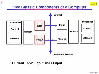
Datapath And in Conclusion… Single cycle control • 5 steps to design a processor • 1. Analyze instruction set => datapath requirements • 2. Select set of datapath components & establish clock methodology • 3. Assemble datapath meeting the requirements • 4. Analyze implementation of each instruction to determine setting of control points that effects the register transfer. • 5. Assemble the control logic • Control is the hard part • MIPS makes that easier • Instructions same size • Source registers always in same place • Immediates same size, location • Operations always on registers/immediates Processor Input Control Memory Output