Download
1 / 17
170 likes | 184 Vues
An Introduction to Silego's Ultra Low R DSON Integrated Power Switches. November 2016 v.1.0. Silego Integrated Power Switch (IPS) Categories. Silego Integrated Power Switch Advantages. Proprietary CuFET ™ Technology Ultra low R DSON

E N D
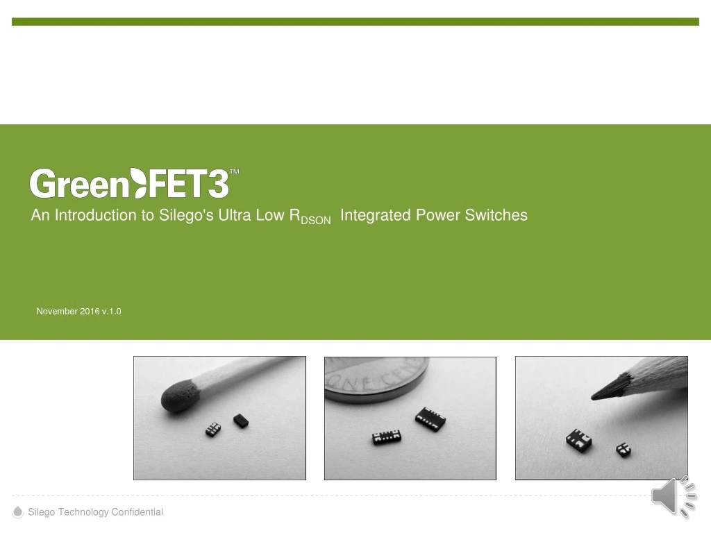
An Introduction to Silego's Ultra Low RDSON Integrated Power Switches November 2016 v.1.0
SilegoIntegrated Power Switch Advantages • Proprietary CuFET™ Technology • Ultra low RDSON • nFETs: Singles as low as 4 mΩ; Back-to-back (B2B),Reverse-current Block (RCB) as low as 15 mΩ • pFETs: Single/duals as low as 23 mΩ • Ultra-small package sizes: 1mm2 to 4mm2 ST[D/Q]FNs, 0.4mm pitch • Continuous operating currents: 1A to 9A • Greater flexibility in power sequencing • Fixed or adjustable VOUT eliminates “RC” tuning variation controlled inrush current • Faster overall power-up sequencing • Built-in System-level Protection Circuits • Input under/over-voltage protection • Fixed or resistor-adjustable current limit • Short-circuit protection • Thermal shutdown with auto restart • Reverse-current blocking • Logic-level Turn-on Signaling • Eliminates external level shift or charge pump circuitry to drive FET
Silego’s Integrated CuFET™ MOSFETTechnology • Single-die Integration: • Cu-FET™ Technology → Inverted-die packaging → Eliminates bond wires & lead frame • 0.18-µm Control Circuitry + High-IDS/Low RDSON n/p-channel MOSFETs • Foundry Process: Low-voltage IPSs → 3.6V or 5V CMOS Logic 24V High-voltage IPSs → 5V CMOS Logic + High-voltage Add-on Module Low sheet ρ interconnects Drain Source Octagonal FET “Cell” Top-side Redistribution Layer Control Circuit Gate Metal Layers& Vias FET Array Gate Channel Channel Optimal Range:1A ≤ IDS ≤ 10A 20mΩ RDSON ~100,000 FET “cells” Note: Not to scale
Silego’sIntegrated CuFET™ MOSFETTechnology (for Flip Chip) TDFNLead Frame Low sheet ρ Cu pillars 0.55mm Plastic package encapsulant Note: Not to scale
Single-channel Integrated Power Switch MOSFET Circuit + Discharge Circuit An ultra Low RDSON Single-channel Integrated Power Switch, 1.5x 2.0 mm package
Typical Block Diagram of Single-channel nFET IPS Proprietary CuFET™ technology for very low RDSON Continuous IDS Capacitor for adjusting VOUT slew rate and inrush current control • Downstream Load Details: • FPGA or application processor • LCD Display • BT Radio or WLAN • USB or Powered ports • Buck/Boost converter or LDO • HV fan motor (inductive load) Resistor for adjusting Active Current Limit threshold 1.6 x 2.5 x 0.55 mm 16 pin
Typical Block Diagram of Single-channel pFET IPS Continuous IDS 1.0 x 1.0 x 0.55 mm 4 pin SLG59M1557V SLG59M1558V
Dual-channel nFETIntegrated Power Switch ≥4mm2 ≥4mm2 MOSFET Channel 2 Circuit MOSFET Channel 1 Circuit Discharge Channel 1 Discharge Channel 2 Discrete Solution: ≥24mm2 + 0402 Rs & Cs Silego Solution: 1.6mm2 incl’g protection ckts Dual-channel Power Switch in a 1.0 x 1.6 mm Package
Typical Block Diagram of Dual-channel nFET IPS ILOAD1 ILOAD2 1.0 x 3.0 x 0.55 mm 14 pin SLG59M1527V SLG59M1603V SLG59M1612V
Typical Block Diagram of Dual-channel pFET IPS 1.0 x 1.6 x 0.55 mm 8 pin SLG59M1638V SLG59M1639V SLG59M1640V SLG59M1641V
Typical Block Diagram of Single-channel nFETIPS with Reverse Blocking Feature ILOAD 1.5 x 2.0 x 0.75 mm 8 pin SLG59M610V SLG59M1563V SLG59M1600V SLG59M1714V
GreenFET3 Over-current Protection If current-limit condition is not triggered, IPS operates in normal mode.Thermal protection is not activated.
GreenFET3 Over-current Protection If current-limit condition is triggered, then thermal protection is activated.
GreenFET3 Short-circuit Protection For short circuit on the VOUT pin – thermal protection is not triggered, output voltage VOUT = 0V and MOSFET is saved from damage.
GreenFET3 VOUT Ramp Rate Conditions: CSLEW = 4 nF; VDD = 5 V; VD = 5 V
Learn more about GreenFET3 products at our website http://www.silego.com/products/greenfet3.html GreenFET3 Product Selector Guide (English) AN-1068 GreenFET3 Integrated Power Switch Basics HFET1 Product Selector Guide