Download
1 / 2
20 likes | 164 Vues
(c). (b). 200nm. 200nm. Materials World Network: Co core HfO 2 shell nanocrystal memory Jianlin Liu, University of California-Riverside, DMR 0807232.

E N D
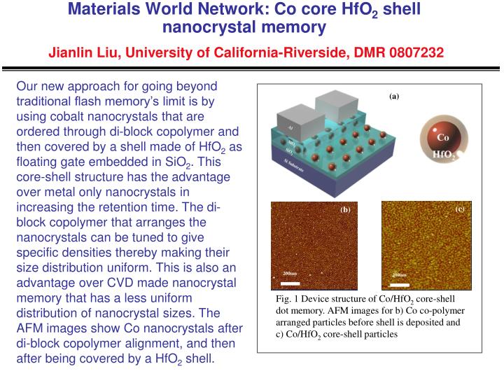
(c) (b) 200nm 200nm Materials World Network: Co core HfO2 shell nanocrystal memoryJianlin Liu, University of California-Riverside, DMR 0807232 Our new approach for going beyond traditional flash memory’s limit is by using cobalt nanocrystals that are ordered through di-block copolymer and then covered by a shell made of HfO2 as floating gate embedded in SiO2. This core-shell structure has the advantage over metal only nanocrystals in increasing the retention time. The di-block copolymer that arranges the nanocrystals can be tuned to give specific densities thereby making their size distribution uniform. This is also an advantage over CVD made nanocrystal memory that has a less uniform distribution of nanocrystal sizes. The AFM images show Co nanocrystals after di-block copolymer alignment, and then after being covered by a HfO2 shell. (a) Fig. 1 Device structure of Co/HfO2 core-shell dot memory. AFM images for b) Co co-polymer arranged particles before shell is deposited and c) Co/HfO2 core-shell particles
Nanotechnology technician trainingJianlin Liu, University of California-Riverside, DMR 0807232 An ongoing effort by the San Bernardino Community College District and UC Riverside is to train the local technician workforce in the skills required to enter the field of nanotechnology. The course development as well as part of the teaching duties fell to the faculty of UCR and the graduate student Mario Olmedo for the first year. The courses taught were introductory to electronic and optoelectronic devices as well as fabrication and characterization techniques. The total course load is 90 hours over a period of about 8 weeks for each run. So far several runs have been completed and an excess of 150 trainees have completed this set of courses. Graduating class of students of the nanotechnology technician training