Download
1 / 13
130 likes | 295 Vues
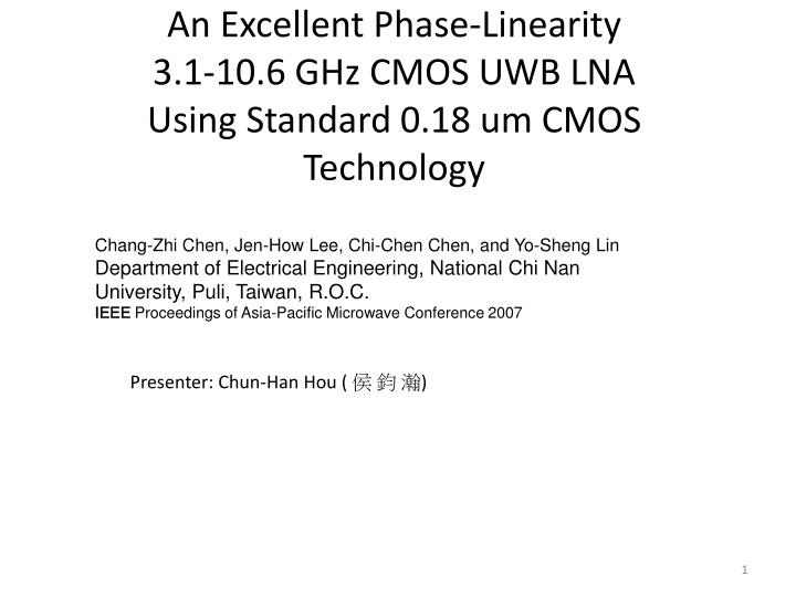
An Excellent Phase-Linearity 3.1-10.6 GHz CMOS UWB LNA Using Standard 0.18 um CMOS Technology. Chang-Zhi Chen, Jen-How Lee, Chi-Chen Chen, and Yo-Sheng Lin Department of Electrical Engineering, National Chi Nan University, Puli, Taiwan, R.O.C.

E N D
An Excellent Phase-Linearity 3.1-10.6 GHz CMOS UWB LNAUsing Standard 0.18 um CMOS Technology Chang-Zhi Chen, Jen-How Lee, Chi-Chen Chen, and Yo-Sheng LinDepartment of Electrical Engineering, National Chi Nan University, Puli, Taiwan, R.O.C. IEEE Proceedings of Asia-Pacific Microwave Conference 2007 Presenter: Chun-Han Hou( 侯 鈞 瀚)
Abstract 1. To achieve high and flat gain and small group-delay-variation at the same time, the inductive peaking technique is adopted in the output stage for bandwidth enhancement. 2. The UWB LNA dissipates 22.7 mW power and achieves input return loss (S11) of -9.7 - -19.9 dB, output return loss (S22) of -8.4 - -22.5 dB,flat forward gain (S21) of 11.4 ± 0.4 dB, reverse isolation (S12) of -40 - -48 dB, and noise figure (NF) of 4.12 - 5.16 dB over the 3.1-10.6 GHz band of interest. 3. Good 1-dB compression point (P1dB) of -7.86 dBm and input third-order inter-modulation point (IIP3) of 0.72 dBm are achieved at 6.4 GHz. The chip area is only 681 um x 657um excluding the test pads.
Outline 1.Introduction 2.LNA Design 3.Measurement Result 4.Conclusion
Introduction 1.UWB low-noise amplifier (LNA) is a critical block in UWB transceiver design. To amplify the small radio signals received from the whole UWB band with good signal-to-noise ratio property, in addition to high and flat S21 and low S11 S22, low and flat noise figure (NF) is also required. 2. To demonstrate that good power and phase linearity performances can be achieved simultaneously for a CMOS UWB LNA, in this work, we demonstrates a high performance 0.18 tm CMOS UWB LNA with good power and phase linearity performances, which is suitable for both OFDM and UWB pulse-radio system applications.
LNA Design • this LNA is composed of a cascoded input-stage and a common-source output-stage. • simultaneous input impedance and noise matching over the 3.1-10.6-GHz-band of interest is achieved by appropriately selecting the values of LG1, Ls1, RF1. • The output of each stage is loaded with a band-pass LC network to provide parallel resonance, i.e. to maximize the gain over the 3.1-10.6-GHz-band of interest. A peaking inductor LG3 is added to the gate-terminal of M3 to increase the 3-dB bandwidth of the output stage.thefeedback • resistorsRF1 and RF3 are also beneficial for the input and output impedance matching, • respectively.
Measurements The die photo of the finished circuit is shown in Fig. I (b). The chip area is only 681 um x 657 um excluding the test pads.
Fig. 2(a) and 2(b) show the measured S11, and S22 versus frequency characteristics of the CMOS UWB LNA, respectively. S11, of -9.7 - -19.9 dB and S22 of -8.4 - -22.5 dB were achieved over the 3.1-10.6-Ghzband of interest. Fig. 2(c) and 2(d) shows the measured S21 and S12 versus frequency characteristics of the CMOS UWB LNA, respectively. High and flat S21 of 11.4±0.4 dB, and good S12 of -40 - -48 dB were achieved over the 3.1-10.6- GHz-band of interest.
Fig. 3 shows the measured group delay versus frequency characteristics of the CMOS UWB LNA. Good phase linearity property is achieved, i.e. group delay variation is only 17.4 ps across the whole band.
1.Fig. 4, this LNA achieved NF of 4.12 - 5.16 dB over the 3.1-10.6-GHz-band of interest. 2.Besides, good P1dB of -7.86 dBm and IIP3 of 0.72 dBm were achieved for the LNA at 6.4 GHz, as shown in Fig. 5.
Conclusion 1.the inductive peaking technique to achieve high and flat UWB S21 and good phase linearity, is implemented. 2. This LNA also exhibits good power linearity, small chip area and power consumption. 3.These results demonstrate that this UWB LNA is very suitable for both OFDM system and UWB pulse-radio system applications.