Download

1 / 8
90 likes | 222 Vues
Carbon Nanotube-Based Nonvolatile Random Access Memory for Molecular Computing. Thomas Rueckes, et al. Science 289 , 94 (2000). Overview. Non-volatile memory can retain the stored information even when not powered.

E N D
Carbon Nanotube-Based Nonvolatile Random Access Memory for Molecular Computing Thomas Rueckes, et al. Science 289, 94 (2000)
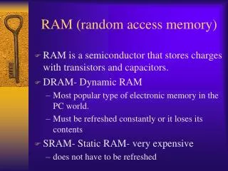
Overview • Non-volatile memory can retain the stored information even when not powered. • Different types of memory: MROM, EPROM, EEPROM, OTP, NAND/NOR Flash, Phase-change, MRAM, etc • NAND Flash is by far the largest percent of all NVM in the market today (Toshiba/SanDisk, Samsung, Hynix)
Single-Walled Nanotube (SWNT) crossbar array Bi-stable electromechanical switch OFF and ON states corresponding to elastic energy at finite separation and van der Waal energy minima Switching between the states is accomplished by transiently charging SWNT to produce attractive and repulsive forces Structure and Principle of Operation “Organic or Inorganic support structure” Metal contact (Paladium?) SiO2 Si substrate van der Waal contact
I-V Characteristics Lower 1,2 Upper 3,4 OFF RON/ROFF ~ 10 ON RON/ROFF ~ 105
ON/OFF state can be detected by measuring the resistance of the junction +V V2 -V +V V1 +V Program/Erase/Read Read Program V=4.5V Erase V=20V
Random distribution of metallic and semiconducting SWNT Crosspoint structure has multiple pathways and would need directional element like diode Growth Issues (according to the authors)
Key Challenges to Practical Applications • Retention—ability to retain stored states for long periods under adverse conditions • Endurance—ability to switch multiple times without degrading performance • Scalability—program/erase voltages • Array Efficiency—user-bits vs. support circuitry
Questions? Thank You!