Download
1 / 2
20 likes | 139 Vues
Synthesis of CCs and CFOAs by manipulation of VFs and CFs. Leticia Torres-Papaqui, Esteban Tlelo-Cuautle INAOE. Department of electronics, MEXICO.

E N D
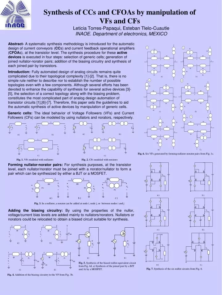
Synthesis of CCs and CFOAs by manipulation of VFs and CFs Leticia Torres-Papaqui, Esteban Tlelo-Cuautle INAOE. Department of electronics, MEXICO Abstract- A systematic synthesis methodology is introduced for the automatic design of current conveyors (CCs) and current feedback operational amplifiers (CFOAs), at the transistor level. The synthesis procedure for these active devices is executed in four steps: selection of generic cells; generation of joined nullator-norator pairs; addition of the biasing circuitry and synthesis of each joined pair by transistors. Introduction: Fully automated design of analog circuits remains quite complicated due to their topological complexity [1]-[2]. That is, there is no simple rule neither to describe nor to establish the number of possible topologies even with a few components. Although several efforts has been devoted to enhance the capability of synthesis for several active devices [3]-[5], the selection of a correct topology along with the biasing problem, constitutes the most complicated part of analog design automation of transistor circuits [1],[6]-[7]. Therefore, this paper sets the guidelines to aid the automatic synthesis of active devices by manipulation of generic cells. Generic cells: The ideal behavior of Voltage Followers (VFs) and Current Followers (CFs) can be modeled by using nullators and norators, respectively. Fig. 6. Six VFs generated by forming nullator-norator pairs from Fig. 1c. Fig. 1. VFs modeled with nullators Fig. 2. CFs modeled with norators Forming nullator-norator pairs: For synthesis purposes, at the transistor level, each nullator/norator must be joined with a norator/nullator to form a pair which can be synthesized by either a BJT or a MOSFET. Fig. 3. In a nullator, a norator can be added at node i, node j, or between nodes i and j Adding the biasing circuitry: By using the properties of the nullor, voltage/current bias levels are added mainly to nullators/norators. Nullators or norators could be relocated to obtain a biased circuit suitable for synthesis. Fig. 5. Synthesis of the biased nullor equivalent circuit from Fig. 4d. a) Synthesis of the joined pair by a BJT and, b) by a MOSFET. Fig. 7. Synthesis of the six nullor circuits from Fig. 6. Fig. 4. Addition of the biasing circuitry to the VF from Fig. 3b.
Synthesis of CCs and CFOAs by manipulation of VFs and CFs Leticia Torres-Papaqui, Esteban Tlelo-Cuautle INAOE. Department of electronics, MEXICO Fig. 7. Four CFs generated by forming nullator-norator pairs from Fig. 2c. Fig. 8. Synthesis of the four nullor circuits from Fig. 7. Synthesis of the CC by superimposing one VF and one CF. Synthesis of the CFOA by cascading one CC and one VF. Acknowledgment: This work is supported by CONACyT-MEXICO under project J40321-Y. CONCLUSION: It has been introduced a systematic synthesis methodology focused on the automatic design of active devices at the transistor level. It has been shown that this methodology is well suited to generate new transistor circuits. The proposed synthesis method has been divided in four steps: selection of a generic cell implemented with nullators or norators, the manner in which an automatic system adds nullators or norators to form joined pairs suitable for biasing purposes, the manner in which an automatic system adds the biasing circuitry, and the manner in which each joined pair is synthesized by a BJT or a MOSFET. Optimization techniques must be applied to the generated designs in order to obtain the better behavior and performance of the final transistor circuit design. Finally, the method has been highlighted by synthesizing the CC and CFOA, for which SPICE simulation results show the suitability and capability of the proposed technique to generate novel active devices. REFERENCES [1] R.A. Rutenbar, G.E. Gielen, B.A. Antao, Computer-Aided Design of Analog Integrated CAS, IEEE Press NJ (2002) [2] C. Toumazou, B. Gilbert, G. S. Moschytz, Trade-Offs in Analog Circuit Design, Kluwer Academic Pub. London (2002) [3] H. Schmid, Approximating the universal active element, IEEE TCAS-II, vol. 47, no. 11 (2000) 1160-1169 [4] Hajime Shibata and Nobuo Fujii, Analog circuit synthesis by superimposing of sub-circuits, IEEE ISCAS, vol. V (2001) 427-430 [5] D. Haigh, F.Q. Tan, Christos P., Systematic synthesis method for analogue circuits, IEEE ISCAS, vol. I (2004) 709-712. [6] E. Tlelo, A. Diaz, An heuristic circuit-generation technique for the analog design-automation, IEEE ISCAS, vol. I (2003) 193-196. [7] Tlelo-Cuautle E., Computing the elements embedded into a positive feedback loop, IEEE ISCAS, vol. III (2002) 531-534. [8] E. Tlelo, et al., SIASCA: Interactive system for the symbolic analysis of analog circuits, IEICE Elex, vol. 1, no. 1 (2004) 19-23 [9] Aguila J., Torres L., Tlelo E., Improving symbolic analysis in CMOS analog circuits, IEEE ISCAS, vol. V (2004) 193-196. [10] J. Sheldon, X. Tan, Behavioral Modeling of Analog Circuits by Dynamic Semi-Symbolic Analysis, IEEE ISCAS, V (2004) 105-108. [11] K.Laker, W.Sansen, Design of Analog Integrated CAS, McGraw-Hill (1994)