Download
1 / 25
250 likes | 369 Vues
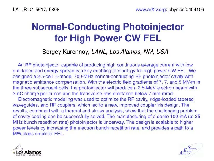
LA-UR-04-5617,-5808. www.arXiv.org : physics/0404109. Normal-Conducting Photoinjector for High Power CW FEL.

E N D
LA-UR-04-5617,-5808 www.arXiv.org: physics/0404109 Normal-Conducting Photoinjector for High Power CW FEL An RF photoinjector capable of producing high continuous average current with low emittance and energy spread is a key enabling technology for high power CW FEL. We designed a 2.5-cell, p-mode, 700-MHz normal-conducting RF photoinjector cavity with magnetic emittance compensation. With the electric field gradients of 7, 7, and 5 MV/m in the three subsequent cells, the photoinjector will produce a 2.5-MeV electron beam with 3-nC charge per bunch and the transverse rms emittance below 7 mm-mrad. Electromagnetic modeling was used to optimize the RF cavity, ridge-loaded tapered waveguides, and RF couplers, which led to a new, improved coupler iris design. The results, combined with a thermal and stress analysis, show that the challenging problem of cavity cooling can be successfully solved. The manufacturing of a demo 100-mA (at 35 MHz bunch repetition rate) photoinjector is underway. The design is scalable to higher power levels by increasing the electron bunch repetition rate, and provides a path to a MW-class amplifier FEL. Sergey Kurennoy, LANL, Los Alamos, NM, USA
Normal-Conducting RF Photoinjector • Requirements: • CW, 700-MHz RF; emittance < 10 mm·mrad at the wiggler • 3 nC per bunch, 100 mA at 35-MHz bunch rep rate (→ 1 A) • Design: • split cavities: 2.5-cell PI (old 777 design: 7,7,7 MV/m, 2.70 MeV → new 775 design: 7,7,5 MV/m, 2.54 MeV) + booster (4 cells, 4.5 MV/m, 5.5 MeV) • PI: 2.5 cells, emittance-compensated, on-axis electric coupling • 100 mA: Pw (668 kW) + Pb (254 kW) → 1 A: 668 kW + 2540 kW • EM modeling: cavity, RF couplers, and ridge-loaded tapered waveguides • Beam dynamics – TS2 versus Parmela • Thermal & stress analysis, manufacturing → AES, Medford, NY High Average Power Workshop, UCLA. November 8-10, 2004
2.5-cell RF Photoinjector Cavity Magnets Vacuum plenum Cavity MAFIA model of 2.5-cell cavity with magnets and vacuum plenum High Average Power Workshop, UCLA. November 8-10, 2004
2.5-cell RF Photoinjector Cavity 2.5-cell PI with vacuum plenum – SF & MAFIA results High Average Power Workshop, UCLA. November 8-10, 2004
Normal-Conducting RF Photoinjector Cooling Photocathode plate Ridged tapered waveguides for RF power input 2.5-cell PI with emittance-compensating magnets (left) and vacuum plenum (right) High Average Power Workshop, UCLA. November 8-10, 2004
NC RF Photoinjector: Microwave Studio Modeling Photo-cathode position On-axis electric field for 777(old) and 775 designs 0 18 MV/m Electric field of p-mode in 2.5-cell cavity: E0=7 MV/m in cells 1&2, 5 MV/m in cell 3. High Average Power Workshop, UCLA. November 8-10, 2004
43 W/cm2 103 W/cm2 17.25 kA/m 0 NC RF Photoinjector: Microwave Studio Modeling For comparison: in the old (777) design 75 W/cm2 in 3rd cell Power in the 775 design: Pw = 668 kW versus Pb = 254 kWfor 100 mA, but Pb = 2540 kWfor 1 A Surface current distribution for thep-mode in 2.5-cell photoinjector cavity (775) High Average Power Workshop, UCLA. November 8-10, 2004
RF Power for NC Photoinjector • 922 kW of RF input power for 100 mA beam current: • CW, 700-MHz RF power is fed through two waveguides • Ridge-loaded tapered waveguides (RLWG) • Design is based on LEDA RFQ and SNS power couplers • Ridge profile is found by SF calculations for cross sections (LY), and checked using MicroWave Studio (MWS) 3-D calculations • “Dog-bone” shaped RF coupling irises Transition section from full-height WG1500 to half-height WG1500 Ridge-loaded tapered waveguide High Average Power Workshop, UCLA. November 8-10, 2004
EM Modeling of RF Coupler General layout of the model “Dog-bone” iris of RF couplers Half-height WG 1500 Ridge-loaded tapered waveguides for RF input RF coupler model. Tapered ridge-loaded waveguides are coupled to the 3rd cell of photoinjector cavity (modeled here by a pillbox) via irises cut through thick walls. High Average Power Workshop, UCLA. November 8-10, 2004
EM Modeling of RF Coupler Details of coupler irises R 19 mm 2″ “Dog-bone” iris of RF couplers Ridge-loaded tapered waveguide & iris Hole Ø 9.5 mm RF coupler model. Details of coupler irises and ridge-loaded tapered waveguides. The wall thickness near the iris is 1.2″, the iris gap width is 1.8 mm. High Average Power Workshop, UCLA. November 8-10, 2004
The required WG-cavity coupling is For the pillbox model, the required coupling is Then the required Qe for the model is EM Modeling of RF Coupler Procedure We calculate Qe in the model directly using time-domain simulations with MicroWave Studio (MWS), and adjust the coupling. After that, again in MWS, an RF signal with a constant amplitude is fed into waveguides to find the match point (Pout = 0), and calculate the field and surface power distributions at the match. S.S. Kurennoy, L.M. Young. “RF Coupler for High-Power CW FEL Photoinjector”, PAC2003, p. 3515. High Average Power Workshop, UCLA. November 8-10, 2004
EM Modeling of RF Coupler: Time Domain (TD) • MWS time-domain • calculations: • Determine Qe • Find match point Match point for Ibeam = 100 mA: Pout= 0 Amplitudes of: RF input signal Output signal Thermal test point: Ibeam= 0 Pout= 0.025Pin High Average Power Workshop, UCLA. November 8-10, 2004
From energy balance one can find power ratio where EM Modeling of RF Coupler Coefficient 0<a<1 is the amplitude ratio of the input and reflected waves, 1-a<<1. For b = 1, bc = 1.38, ratio Pout/Pin ≈ 0.025, practically independent of value of a. For a= 1, (1-x)2/(1+x)2; a= 0.99; a= 0.95; a= 0.90. • High Average Power Workshop, UCLA. November 8-10, 2004
EM Modeling of RF Coupler: TD Results Maximal power density is 120 W/cm2 at 461 kW RF input power per waveguide Regions with high power density are well localized → separate cooling Fields values are for 0.5 W RF input power and should be scaled by factor 960 Surface magnetic fields at the match point from MWS time-domain simulations High Average Power Workshop, UCLA. November 8-10, 2004
EM Modeling of RF Coupler: TD Results Maximal power density is 120 W/cm2 at 461 kW RF input power per waveguide Fields values are for 0.5 W RF input power and should be scaled by factor 960 Surface currents near the irises at the match from MWS time-domain simulations High Average Power Workshop, UCLA. November 8-10, 2004
EM Modeling of RF Coupler: TD Results Maximal power density is 120 W/cm2 at 342 kW RF input power per waveguide Max power density is the same as for the 100-mA match point Fields values are for 0.5 W RF input power and should be scaled by factor 827 Surface currents near the irises at thermal-test point (no beam, 2.5% reflection) High Average Power Workshop, UCLA. November 8-10, 2004
EM Modeling of RF Coupler: Eigensolver X-check Fields values should be scaled by factor 0.636 Maximal power density 120 W/cm2 Surface currents from MWS eigensolver calculations (mesh 3.006M for 1/8) High Average Power Workshop, UCLA. November 8-10, 2004
EM Modeling of RF Coupler: Results for 775 MWS time domain MWS eigensolver Compare to 43 W/cm2 at smooth wall in the 3rd cell far from irises: power ratio is < 2.8 → field enhancement due to irises is < 1.65 For 777 design max dP/dswas220 W/cm2 * W/o beam, 342 kW per WG (incl. 2.5% reflection) For reference: in the LEDA RFQ couplers max dP/ds≈ 150 W/cm2, while the power ratio (max / smooth wall) was about 10 Maximal values of surface power density from MWS calculations High Average Power Workshop, UCLA. November 8-10, 2004
NC Photoinjector, RF Couplers :Summary • 100-mA operation of normal conducting photoinjector requires almost 1 MW of CW 700-MHz RF power that will be fed through two ridge-loaded tapered waveguides. • RF coupler design is based on LEDA RFQ and SNS couplers. The coupler-cavity system is modeled using a novel approach with direct MWS time-domain simulations. Results for the maximal power density are checked using eigensolvers. • The coupler design is optimized using 3-D EM modeling to reduce the maximal surface power density on the coupler irises: • Increased hole radius and wall thickness; blended iris edges; • Field enhancement is only 65% compared to smooth cavity walls. • In the 775 PI cavity, the max power density near the irises is only 15% higher than max in the smooth cavity. This design reduces stresses and facilitates cavity cooling. Thermal management is still challenging but feasible. • The PI cavity is being manufactured by AES. Its thermal tests with full RF load are scheduled at LANL (LEDA) in 2005. High Average Power Workshop, UCLA. November 8-10, 2004
RF Cavity Model with 4 RLWG: Matched at 0.46 A Maximal power density is 120 W/cm2 at 461 kW RF input power per waveguide Fields values are for 0.5 W RF input power and should be scaled by factor 960 Surface currents at the match point from MWS time-domain simulations High Average Power Workshop, UCLA. November 8-10, 2004
2.5-cell Photoinjector:Beam Dynamics Transverse rms beam size, mm Norm. transverse rms emittance Parmela simulations of 2.5-cell PI + booster + linac (L. Young) High Average Power Workshop, UCLA. November 8-10, 2004
2.5-cell Photoinjector:Beam Dynamics Comparison of MAFIA TS2 and Parmela results for 3-nC bunch charge High Average Power Workshop, UCLA. November 8-10, 2004
2.5-cell Photoinjector:Beam Dynamics 3 nC 10 nC MAFIA TS2 simulations of 2.5-cell PI (wake fields included) High Average Power Workshop, UCLA. November 8-10, 2004
2.5-cell Photoinjector:Beam Dynamics 10 nC, E-scale is fixed MAFIA TS2 simulations of 2.5-cell PI: 10-nC bunch charge High Average Power Workshop, UCLA. November 8-10, 2004
Beam dynamics in photoinjector:Summary • 100-mA operation of the normal-conducting 700-MHz CW photoinjector requires 3-nC bunches at 35-MHz bunch repetition rate. Higher currents are achievable with higher bunch repetition rates. • Beam dynamics in the PI RF cavity is modeled using Parmela and MAFIA TS2 particle-in-cell (PIC) simulations. Results for 3 nC are in agreement. • Wake fields effects are weak, even for 10 nC. TS2 simulations with multiple bunches at 350-MHz repetition rate show identical parameters of bunches at the cavity exit. • The PI cavity is being manufactured by AES. Its thermal tests with full RF load are scheduled at LANL (LEDA) in 2005. High Average Power Workshop, UCLA. November 8-10, 2004