Download
1 / 27
270 likes | 280 Vues
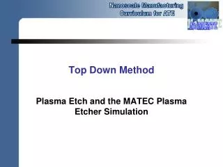
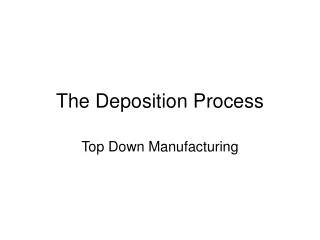
Top Down Method The Deposition Process.

E N D
Top Down MethodThe Deposition Process Author’s Note: Significant portions of this work have been reproduced and/or adapted with permission from material created by the Maricopa Advanced Technology Education Center, part of the Academic Affairs Division, Maricopa Community College District.
Learning Objectives • The Student Will Be Able to Explain • The need for Deposition Processes in the Top Down Manufacturing Process • The methods used to perform physical and chemical deposition processes • The advantages of different deposition processes • The use of plasma for enhancing deposition
Purpose of Deposition • Deposition places conductive or insulating layers on a substrate • Deposition processes create locally conductive paths that can be used to interconnect devices • Deposition can be used to build up more complex structures one layer at a time
Deposition Types • Silicon Dioxide SiO2 • Insulating layers • Protective coatings • Gate oxides • Silicon Nitrides • Protective layers • Isolation
Deposition Types • Polysilicon • Heavily doped silicon • Conductive • Used for interconnects and gate • Metals • Aluminum/Aluminum-Copper • Tungsten • Titanium Alloys
Deposition Processes • Physical or Chemical (or both?) • Physical Processes Deposit the material without chemical reactions • Chemical processes utilize liquid or vapor forms of precursors that react with the surface to form the desired deposition • It is possible to combine the processes and gain the benefits of each • Many processes are carried out in reduced pressure (partial vacuum) environments
Requirements of Deposition • Since top-down processes may use many layers to form a product, any deposited layer must be compatible in many ways with what is below it • Film Stress • Conformality • Uniformity • Step Coverage • Thermal compatibility
Result of Non-Uniform Deposition From MATEC Module 61
Conformal Coverage Good Conformal Coverage Poor Conformal Coverage From MATEC Module 54
Step Coverage From MATEC Module 54
Physical Deposition Processes • Sputtering • Plasma is created by RF or HV DC source • Inert gas such as Ar is used in a low pressure environment • Free electrons strike Ar atoms, causing positive ions to be formed • Negatively charged target material attracts ions • Ions dislodge particles that are deposited
Practice Questions Click once for each question. 1. What are the two main types of deposition processes? Physical and Chemical Deposition 2. What are commonly used metals for deposition? Aluminum, tungsten, and copper 3. What does conformality of a deposition refer to? The ability of the deposition to follow surface contours evenly
Sputtering Source: www.wikipedia.com
Sputtering (3) • Advantages • Low temperature process • Good Conformal Coating • Good Step Coverage • Disadvantages • Dielectrics require RF Source • RF environment may affect other depositions
Evaporative Deposition • Utilizes the principle of vapor pressure • Metallic species are melted in a low pressure environment • Higher vapor pressure metals evaporate first • Deposition of the vapor on the surface occurs • A low temperature process on the substrate • Alternatives include laser ablation • Laser strikes a target, causing local melting
Evaporative Deposition (2) • Advantages • Uniformly covers substrate • Simple process without chemicals or gases • Disadvantages • Alloys are difficult to deposit • Different metals have different vapor pressures • High aspect ratio features are difficult to cover • Trajectory of evaporated particles tends to be vertical, which may not pattern sidewalls evenly
Practice Questions Click once for each question. 1. Which physical deposition process uses plasma? Sputtering 2. What is an advantage of sputtering? Low temperature process, good conformal coating 3. What is a disadvantage of evaporative deposition? Difficult to deposit alloys, difficult to get good high aspect ratio feature deposition
Spin On Coating • A Physical Deposition Process • Similar to photoresist spin-on • Si-based liquid is applied • Coating is baked on to remove volatile liquid • Used to planarize or flatten wafer surface • Can be patterned and etched for contacts • Adds steps to process • Alternatives – Chemical Mechanical Polish (if the objective is only to planarize surface)
Chemical Deposition Processes • Wet or Dry? • Wet processes use liquids and immersion • Electroplating • Electroless deposition • Wet growth of SiO2 insulating layer (water vapor) • Dry processes use chemical vapors • Atmospheric Pressure Chemical Vapor Deposition • Low Pressure Chemical Vapor Deposition • Plasma Enhanced Chemical Vapor Deposition
Chemical Deposition Processes • Atmospheric Chemical Vapor Deposition (CVD) • Wafers are heated • Chemical gases are introduced • A temperature dependent deposition rate • Mass transport limited at higher temperatures From MATEC Module 54
Chemical Deposition Processes • Low Pressure (CVD) • Surface reaction limited at low pressure • Chamber may also be heated or unheated • Low pressure environment increases mean free path • Better Step Coverage and uniformity than APCVD From MATEC Module 54
Chemical Deposition Processes • Plasma Enhanced Low Pressure (CVD) • Lower Temperature Process due to Plasma Enhancement • Dissociation of precursor gas molecules (Homogeneous reactions) • Ions bombard surface making it more reactive • Higher rates of deposition are possible than with LPCVD From MATEC Module 54
Chemical Deposition Processes • Anti-reflective coatings • Reflection from shiny layers below photoresist causes blurred features • Utilize thin film deposition to create coatings that have λ/2 thickness at the exposure lamp wavelength • This results in destructive interference canceling reflection in the photoresist layer • Finer lithography is possible
Practice Questions Click once for each question. 1. What are the advantages of atmospheric CVD? Simple equipment requirements and batch processing is possible 2. What is an advantage of low pressure CVD? Improved purity of deposition and good step coverage 3. What is a principal advantage of plasma enhanced CVD? It is a lower temperature process than LPCVD
New Methods for Nanomanufacturing • Thinner layers are necessary for higher speed transistors in IC design • Gate oxide thickness < 50 A • Approaches atomic layer dimensions • Atomic Layer Deposition • A 2 step process of deposition and re-layering • SiOH* + SiCl4 →Si –O-SiCl3 + HCl • SiCl* + H2O → SiOH* + HCl
New Methods for Nanomanufacturing • Molecular vapor deposition • Anti-stiction layers in MEMS are needed to avoid structures fusing to substrates • Vapor deposition of compounds avoids contamination found in liquid processes • Oxygen plasma clean operation precedes deposition process
LIGA Process • LIGA includes X-Ray lithography, electroforming, and plating operations that construct high aspect ratio features on substrates • Precision patterning of a deposited PMMA resist layer using X-Ray lithography • Areas remaining after development are plated with metal • Photo resist and excess metal removed • Remaining features are high aspect ratio metal