Download
1 / 28
290 likes | 458 Vues
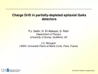
Charge Drift in partially-depleted epitaxial GaAs detectors. P.J. Sellin, H. El-Abbassi, S. Rath Department of Physics University of Surrey, Guildford, UK J.C. Bourgoin LMDH, Université Pierre et Marie Curie, Paris, France. Overview. Chemical reaction growth of thick epitaxial GaAs layers

E N D
Charge Drift in partially-depleted epitaxial GaAs detectors • P.J. Sellin, H. El-Abbassi, S. Rath • Department of Physics • University of Surrey, Guildford, UK • J.C. Bourgoin • LMDH, Université Pierre et Marie Curie, Paris, France
Overview • Chemical reaction growth of thick epitaxial GaAs layers • Depletion thickness and residual impurity concentration • Performance of partially depleted detectors • C-V measurements of impurity concentration at low temperature • Optical probing of charge transport using a focussed laser
Potential challenges for epitaxial GaAs • Strengths of epitaxial GaAs: • intermediate photon detection efficiency between Si and CZT/CdTe • metal-semiconductor contacts and device physics are well understood • epitaxial GaAs has low concentrations of native EL2 defect • source of highly uniform whole wafer material, compatible with flip-chip bonding and monolithic electronics • Existing problems: • even high purity epitaxial is compensated due to residual impurities- does not exhibit intrinsic carrier concentrations • depletion thickness is severely limited • charge carrier lifetimes are reduced
Chemical Reaction growth of thick epitaxial GaAs • Epitaxial GaAs material studied in this work was grown by a Chemical Reaction Method by Jacques Bourgoin (Paris). • An undoped GaAs wafer is used as the material source, which is decomposed in the presence of high temperature high pressure water vapour to produce volatile species. • Typically, growth rates of <10 mm/hr are used to achieve EL2 concentrations of ~1013 cm-3 L. El Mir, et al, “Compound semiconductor growth by chemical reaction”, Current Topics in Crystal Growth Research 5 (1999) 131-139.
Whole wafer photoluminescence mapping • GaAs material uniformity is characterised using room temperature photo-luminescence mapping - a contact-less, whole wafer technique: • A 25 mW 633 nm HeNe laser is focussed to ~50 mm on the wafer • the wafer is mounted on an XY stage, and scanned • PL intensity maps at peak the band edge emission wavelength (870 nm) are acquired
PL maps of GaAs • Photoluminescence mapping clearly shows the uniformity of epitaxial GaAs compared to semi-insulating VGF material: Epitaxial GaAs Bulk GaAs H. Samic et al., NIM A 487 (2002) 107-112.
Calculated depletion thickness • This material is nominally 1-5 x 1014 cm-3- corresponds to a 10-20 mm depletion thickness @ 30V, and 15-30 mm @ 80V
V = 30V V = 80V Alpha particle spectra • 5.48 MeV alpha particles are irradiated through the Schottky (cathode) contact - range in GaAs ~20 mm. • A peltier cooler controlled the device temperature in the range +25°C to -55°C. Shaping time = 0.5 ms.
Alpha particle pulse shapes • Alpha particle pulses at room temperature: time base = 1ms per division fast component preamplifier slow component shaping amplifier
Alpha particle tracks • An un-collimated alpha particle source produces a characteristic ‘double peak’ pulse height spectrum if the depletion thickness is shallower than the particle range:
59.5 keV gamma spectra • Depth-dependent CCE produces poorly resolved gamma spectra: T = -50°C
Temperature dependent CV analysis Allows the doping density ND to be extracted from the gradient of 1/C2 vs V :
Impurity Densities The CV analysis confirm the shallow depletion thicknesses achieved in these devices, and correspond to impurity densities of ~3 x 1013 cm-3 in sample S16 at low temperature:
Focussed IR laser scans Probe the variation in pulse shape as a function of position from the Schottky contact, and temperature
imaging camera cryostat 850nm laser 300ns pulse XY scanning table Scanning optical bench
Laser pulse shapes • T=273K, 20V • At 60mm from cathode: • no slow component to signal • At 180mm from cathode: • charge drift times are ~350ms • IR laser spot appears to have significant beam waist
Laser pulse shapes (2) • T=223K, V=90V • At 60mm from cathode: • no slow component to signal • At 180mm from cathode: • charge drift times are ~350ms • IR laser spot appears to have significant beam waist
Conclusions • The epitaxial GaAs layers studied showed excellent uniformity, and a residual impurity concentration of 1-5 x 1014cm-3 • Long electron lifetimes > 300 ms were observed in the low field regions - confirms the very low EL2 concentration • Lateral laser scans show: • good charge transport in the shallow depleted region • long-lived components to the pulse shapes when irradiated close to n+ substrate - consistent with slow electron diffusion towards the substrate • significant penetration of the depletion region when cooled to -50°C • Future work: • further lateral scanning is required with focussed lasers and high resolution proton microbeams to quantify these phenomena • further modest reductions in impurity concentration will produce significant performance improvements
Acknowledgements • This work was partially funded by the UK’s Engineering and Physics Science Research Council
Figure 3: a spectra at room temperature, as a function of bias. Alpha particle spectra • Epitaxial GaAs pad detectors were irradiated with an uncollimated 241Am alpha particle source. The detector was mounted in a vacuum cryostat, attached to a peltier cooler to allow operation in the temperature range of +25°C to -55°C. Pulse height spectra (figure 3) were acquired using a conventional charge integrating preamplifier and spectroscopy amplifier (shaping time = 0.5ms).