Download
1 / 34
500 likes | 1.24k Vues
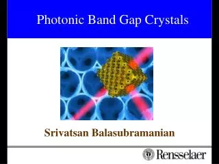
Nanophotonics Class 3 Photonic Crystals. Definition: A photonic crystal is a periodic arrangement of a dielectric material that exhibits strong interaction with light. Examples:. 1D: Bragg Reflector 2D: Si pillar crystal 3D: colloidal crystal. 1D Photonic Crystals.

E N D
Nanophotonics Class 3 Photonic Crystals
Definition: A photonic crystal is a periodic arrangement of a dielectric material that exhibits strong interaction with light
Examples: 1D: Bragg Reflector 2D: Si pillar crystal 3D: colloidal crystal
1D Photonic Crystals Bragg mirror Antireflection coatings (Fresnel equations) Bragg’s law:
Dispersion relation n1: high index material n2: low index material standing wave in n2 n1 n2 n1 n2 n1 n2 n1 frequency ω bandgap standing wave in n1 0 π/a wave vector k
Bloch waves modified slide from Rob Engelen
frequency ω -π/a 0 π/a wave vector k Bloch wave with wave vector k is equal to Bloch wave with wave vector k+m2p/a: This is called the first Brillouin zone modified slide from Rob Engelen
Band diagrams and group velocity of light A light pulse with a center frequency w propagates with group velocity vg, which is altered near the band gap
Example Dielectric mirror 400 – 900 nm Dichroic filters Examples from Thorlabs
1D “photonic crystal” waveguide Joannopoulos et al.
Structure morpho butterfly wing Mode calculation by Gralak et al.
Density of optical states in photonic crystals Band gap: no propagation possible at that frequency: Density of optical states (DOS) is 0
Field propagation into 2D photonic crystal -M direction, TM polarization dielectric band inside bandgap air band Mode calculation with FEMLAB by Aarts TUE.
Bandstructure for two polarizations TM TE Photonic bandgap
2D Photonic Crystals Simulations on a 90° bend in a 2D photonic crystal waveguide. A.Mekis et al., PRL 77, 3787 (1996)
Photonic crystal waveguides Joannopoulos et al.
2D Silicon photonic crystal waveguide bend Zijlstra, van der Drift, De Dood, and Polman (DIMES, FOM)
neff 1.7 Si n 1.5 SiO2 Si Silicon-on-insulator (SOI) Si SiO2
2D Photonic Crystal: holes in semiconductor dielectric 0.35 crystalmodes c/a) p } 0.3 waveguidemodes (units 2 w 0.25 crystalmodes frequency 0.2 0.15 0 0.1 0.2 0.3 0.4 0.5 wavevector |k| (units 2 p /a) H. Gersen et al., PRL 94, 073903 (2005) Kobus Kuipers group at AMOLF
Phase sensitive near-field microscopy developed by Kobus Kuipers et al 500nm Aperture:~200 nm Local measurement of amplitude AND phase. Balistreri et al., PRL 85 294 (2000)
Slow light photonic crystalwaveguide Scansize : 199.8 x 8.1 mm2 pulses : 123 fs, l = 1310 nm • Time resolved motion through a W3 waveguide • Group velocity < c/1000 PRL 94, 073903 (2005) Kobus Kuipers group at AMOLF
3D Photonic Crystals • Woodpile structures • Colloidal crystals • Inverse opals • Focused Ion Beam • ... Photonic Bandgap: No propagation of light with frequencies within the bandgap for three directions ! S.Y. Lin et al, Nature 394 (1998) 251 W.L. Vos [AMOLF]
Infiltrated colloidal crystal: - silica colloidal crystal - infiltration with polystyrene - etching of silica Colvin, MRS Bulletin 26, (2001)
Colloidal photonic crystals Colvin, MRS Bulletin 26, (2001)
Three-dimensional Si photonic crystal Y. A. Vlasov et al., Nature 414, 289 (2001) S.-Y. Lin et al., Nature 394, 251 (1998)
Superstructure in Si woodpile photonic crystal p-polarization, = 20° “zone-folding” M.J.A. de Dood et al. Phys. Rev. B 67, 035322 (2003)
2d and 3D photonic crystals in III-V semiconductors science fiction: lasers, modulators, bends, point defects integrated Noda, MRS Bulletin 26, (2001)
Line defect and point defects in 2D photonic crystals: - photon trapping and emission Joannopoulos et al. Noda, MRS Bulletin 26, (2001) Stoffer et al.