Download
1 / 7
70 likes | 293 Vues
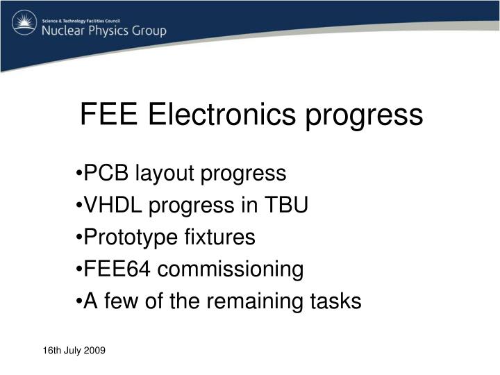
FEE Electronics progress. PCB layout progress VHDL progress in TBU Prototype fixtures FEE64 commissioning A few of the remaining tasks. PCB Layout Progress. June 9 th : 77% signals routed. July 14 th : 100% signals routed. Check :- Impedance matched traces are up to latest spec.

E N D
FEE Electronics progress PCB layout progress VHDL progress in TBU Prototype fixtures FEE64 commissioning A few of the remaining tasks
PCB Layout Progress June 9th : 77% signals routed July 14th : 100% signals routed • Check :- • Impedance matched traces are up to latest spec. • Layout conforms to design rules. • Schematics for undriven signals • Design requirements are met ( run Design Rules Check ) • Board is manufacturable. • Assembly assist marks and information.
PCB progress targets • July 14th : • Completed routing and layout. • July 20th : • Submit to manufacturer for validation and quote. • Submit to assembler for evaluation of assembly and final parts purchase. • July 27th : • Complete engineering review. • Submit to pcb manufacturer and assembler. • September 14th : • Assembled FEE64 delivered.
Collaboration with Detector Systems Development Group (DSDG) of TBU.(Technology Business Unit ) Completed : • Gbit data rate from memory on the devkit => 240Mbit/sec . • System boots with fallback to golden copy. • Created a DMA peripheral with transfer rate of 1.1Gbytes/sec. • Pin allocation of FEE64 memory and Gbit signals checked. Next steps : • Create a memory test and configuration system. • Review the FEE64 schematic and pcb layout.
Prototype fixtures for softwareand VHDL development • Pin out and advice provided by Steve Thomas. • Fixture will allow communications between the ASIC and Linux to be developed. • Mux readout logic VHDL can also be developed. • Fixture designed and manufactured in DL electronic workshops. • 2 ASICs delivered. • Multiplex readout ADC circuit prototype in development for VHDL and performance testing. Fixture comprises a ZIF socket on a pcb designed to mount a packaged ASIC onto an ML507 FPGA development board. Also a copy of the ADC and buffers used for the Multiplex readout.
Initial testing of FEE64 • Power supplies – 28 : Check for noise, stability, accuracy, efficiency…. • FPGA – • Check configuration via JTAG. • Check processor operates with internal memory and terminal. • Check configuration from EEPROM. • DDR2 Memory • Run test system developed by DSDG. • Check results and optimise access speed for best performance. • Gbit Ethernet • Run test system developed by DSDG. • ASIC communications and discriminator output timing • Analog buffers and ADCs
A few of the remaining Tasks • Design Mezzanine pcb ? • Complete Mechanical design. ( Is waiting for final component heights ) • VHDL for prototype fixtures. • Test documentation. • Commission first FEE64 units • VHDL for first experimental use. • Full Linux processor with peripherals and DMA ( from DSDG work ) • ASIC communications ( from prototype work ) • ASIC multiplexed readout. ( from prototype work ) • Timestamped based on discriminator signals. • Formatted and transferred to processor memory as four time ordered data streams. • FEE64 design documentation. • Prepare for production.