Download
1 / 38
620 likes | 1.33k Vues
Phase Detector/Phase frequency Detector. Kaushik Mazumdar. Overview of presentation. Basic PLL block diagram PD/PFD – characteristics Figures of Merits Broad classification and comparisons among the PD/PFD techniques Issues with PFD design : Dead zone and how to avoid it

E N D
Phase Detector/Phase frequency Detector KaushikMazumdar
Overview of presentation • Basic PLL block diagram • PD/PFD – characteristics • Figures of Merits • Broad classification and comparisons among the PD/PFD techniques • Issues with PFD design : Dead zone and how to avoid it • Design tradeoffs between phase noise, frequency range and dead zone • Blind zone and it’s impact on acquisition time • Different types of PFD- 1. Precharged PFD 2. Dynamic logic based PFD 3. Pass transistor based PFD 4. High speed low power PFD 5. Minimal blind zone PFD 6. Dual PFD • Comparison table • summary
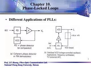
PLL block Diagram Fig 1. PLL
Phase Detector • Compare the phase difference between the input reference signal and the oscillator output signal and its output is a function of the phase difference between the two input signals. • Is a multiplier in Analog PLL • Is formed by logic gates in digital PLL
Digital Phase Detector Texas Instruments Fig 2. PD characteristics
J-K FF based PD Fig 3. J-K FF based PD
Phase Frequency Detector Fig 4. PFD frequency and phase lagging Texas Instruments
Charge pump integrated PFD Fig 5. Charge pump PFD sensitive to only rising edges of ør and øn. Whenever there is rising edge from the output of the R counter, there is the positive transition from the charge pump If the charge pump was sinking current, then it is now in tri state mode. If it was in tri state, then it is now sourcing current. If it was already sourcing current, it continues to do so. Texas Instruments
PFD over PD Average output signal of the PFD varies monotonically with frequency error when PLL is out of lock. δ approaches 1 when w1>>w2’ or w1<<w2’ Δ is nearly .5 when w1>w2’ or w1<w2’,but both frequencies are close together. This characteristics will not be seen in Exor or JK ff based PDs. Since, the output signal of PFD depends on phase Error in the locked state and frequency error in the Unlocked state, a PLL that uses PFD will lock under any condition. Fig 6. Average output signal with change in frequency Texas Instruments
Regions of Operation Fig 7. PLL regions of operation Mike perrott
Design Issues with PFD : Dead Zone Tradeoff between maximum frequency and phase noise Blind zone
Issues with PFD : Dead Zone • Digital PFD exhibit a region of small or zero gain near the phase lock. This low gain region is commonly known as the dead zone. The main cause of dead zone is the relationship between the propagation delay of the internal gates for the reset of the PFD and the switching time of the charge pump currents. • When VCO frequency differs slightly from reference oscillator phase, the PFD should be able to generate short pulse to steer the VCO back to it’s intended frequency. If not, then VCO frequency can fluctuate randomly in that region. Fig 8. Dead Zone [1] No dead zone is important for accurate frequency generation, low phase noise in frequency synthesizer PLL, and low timing jitter in clock generator PLL
Phase characteristics Fig 9. Phase noise spectrum[2] Fig 10. output characteristics of PFD[2] Inside the dead zone, the loop does not suppress the VCO phase noise. Thus the close in phase noise spectrum of the synthesizer equals that of free running VCO In dead zone, the relation between o/p volt and phase error becomes non linear. This deteriorates the close in phase noise of the frequency synthesizer.
How to avoid dead zone Usage of Tri state D-ff based PFD with delay logic added to reset path. The idea is to make the delay in the rest path to be longer than the switching time of the charge pump currents. Fig 11. Tri state PFD [2] Spur: Due to the delay, there will be short pulses both on up and down signal, even when the PLL is in locked state. Thus the charge pump current will switch on and off , and current spikes will appear on the charge pump output at the reference frequency. This will cause reference spurs to appear in the PLL output spectrum.
Tradeoff between reference spurs, Maximum frequency and dead zone [2] The maximum operating frequency of the PFD is derived in soyer’s paper[ ] : Fmax =1/(2xΔTr) Increasing the reset path delay decreases the maximum frequency limit. If ΔTr < Tth , Charge pump cannot close, and there is a dead zone (Where Tth stands for the switching time of the charge pump currents). To avoid dead zone, min delay related to Tth is ΔTrmin = Tth The maximum delay in the PFD reset path is the maximum operating frequency of the PFD which is derived as ΔTrmax =1/(2x Fmax) Lastly, ΔTr has to be made a little longer than ΔTrmin in order to reduce the reference spur
Blind zone • The frequency insensitivity of the PFD to any transitions in the input signals in known as blind zone. This blind zone induces wrong polarity in the PFD output, leading to incorrect behavior and increasing the acquisition time. At high frequency, particularly in the PLLs used for optical communication, this is a major problem. • This blind zone degrades the maximum phase detection range (ømax) of the PFD. ømax =2π(1 – Tr x fin)……….[1] One way is to reduce Tr. But it is not possible to remove reset time. Hence, it is not possible to eliminate blind zone. This will lead to poor frequency sensitivity and low phase detection range.
Missing edge phenomenon A rising edge of the VCO clock arrives far earlier than that of the reference clock, thus the PFD activating the D signal. Suppose a rising edge of the VCO clock arrives during the reset time. As the reset pulse overrides the rising edge, the PDF does not detect this rising edge. Fig 12. Missing edge [3] Hence it does not activate D signal that should be generated for the missing edge. In addition, the PFD activates the up signal when the rising edge of the reference clock arrives later. Therefore, a missing edge makes the PFD output being reversed in polarity, enlarging the acquisition time of the PLL.
Blind zone effect on acquisition time [4] • If the phase difference falls into the blind zone during the frequency acquisition, the PFD delivers incorrect phase information to the charge pump and shifts the phase towards opposite direction, which aggravates cycle slips and elongates frequency pull in time. The increased chance of cycle slips adversely affects the PLL frequency acquisition time and is undesirable in systems such as multiband orthogonal FDM. • The acquisition slows by how often wrong information occurs which depend on Δ ( where Δ= 2π Treset/Tref ). At input frequency of Tref = 2 Treset , the PFD outputs wrong information half the time and fail to acquire frequency lock unconditionally.
Different kinds of PFDs • High speed PFD • Dynamic logic PFD • Pass transistor based PFD • Minimal blind zone PFD • Precharged type PFD • Dual PFD
Low power High speed PFD [5] Idea is to lower the delay by removing the feedback path at a lower power. Fig 13 High speed PFD This PD is an open loop PD The generated signal Lag-comp goes high when both of the inputs are low and goes low when they are high, while it does not change when inputs have different values. The two inputs are passed through delay circuitry to synchronize with lag comp. This design suffer from 2 problems : Dead zone when inputs have small phase difference: Owing to finite rise and fall time resulting from the capacitance seen at “lag-comp", Up and down node, pulse may not find time to reach a logic level.
Phase detection circuit Insertion of delay to modify the PD 2nd problem occurs when phase difference of 2 inputs is 180₀ .Lag component goes high impedance Fig 14. Delay insertion[5] This is a detection circuit to detect 180₀ as shown in the figure. A simple circuit used to generate a narrow pulse at the rising edge of “A”, “A-rise” and another one at falling edge of “B”,”B-fall”. The signal π detect is the desired detection signal that is applied to charge pump to get rid of this π phase difference Fig 15 π detection circuit [5]
Dynamic logic PFD [1] Consists of 2 identical circuits handling each of the 2 inputs. The actual output signal are feedback into the circuit, thus providing reset path without any inherent dead zone. Fig 16 Dynamic PFD [1] Transistor MU1 (MDI) and MU4(MD4) charges or drains the potential of node UI(D1) respectively. The potential in node Ul(D1) drives the potential in node U2(D2) to the correct voltage level through transistor MU5,7(MD5,7). The final potential is decided by the REF/DIV input signal through transistor MU6(MD6). Poor phase detection capability at high input frequency. Maximum frequency capability decreases with power supply. Fig 17 Phase detection versus frequency [1]
Pass transistor based PFD [4] Design similar to dynamic 2 phase master slave pass transistor. When both outputs become high, the slave is reset asynchronously while the master is reset synchronously. Synchronous resetting of the master increases the operating range and reduces the power consumption. Fig 18 Pass transistor based PFD [4]
Minimal blind zone PFD [3] The blind zone is primarily caused by reset process. The effect of Treset can be reduced by adding a delay cell at the inputs. The extra delay cell shifts the leading signal until the reset process ends, so that the PFD can respond to rising edge. To ensure proper operation, Tdelay must be smaller than the reset time Treset in all conditions. If Tdelay >Treset, the input clock pulse that triggers the reset would activate the output after the reset ends, which makes the PFD fail. When the phase difference enters the blind zone, the leading phase is delayed by delay cells, and the output has a constant pulse width. Now the blind zone becomes Treset-Tdelay which can be very close to zero. Fig 19 Minimal blind zone PFD [3]
Precharged Phase detector [6] Aim: Removal of dead zone and high speed Since there is no feedback from output, speed of operation improves. Figure shows waveform for the case when slave lags the reference signal. The pulse width of the up signal is larger then the down signal. In this PFD when the PLL is locked, both up and down signals are active. Therefore the phase offset of the PLL depends on the matching between up and down currents of charge pump. The performance degrades at higher input frequencies and dead zone become comparable to conventional design. Fig 20 Precharged PFD [6]
Dual PFD [7] • Sequential PFD has an unlimited error detection range, but a wider dead zone due to the delay/reset path. • Precharged PFD can be used at higher frequency with better speed result, but they have limited error detection range of -π to π • By combining 2 PFD and 2 CP, their advantages can be combined: • Precharged PFD controls the PLL during the locking process • Sequential PFD controls the PLL during the acquisition process
Sequential PFD If the leading edge of REF precedes the leading edge of FB,the UPC signal is generated and vice versa for FB signal. It has no limit to the error detection range and the capture range of PLL with this PFD is limited by the VCO. But, it has a wide dead zone which translates into jitter The operation speed limit is set by the reset operation and hence they cannot be used for high frequency operation. Fig 21 Sequential PFD [7]
Precharged PFD To overcome speed limitation and to reduce the dead zone, dynamic logic based PFD was designed. Fig shows the UP generating section. By virtue of the precharge scheme, flip flops can be eliminated and high frequency operation can be achieved. This PFD shows abnormal behavior outside the error detection range of –π to π Fig 22 Precharged PFD [7]
Dual PFD+CP based PLL When the phase difference (øin)between REF and FB reaches π during the locking process, the lock checker (LC) signal transits to high level and the LCB signal, which is reverse of LC transits to low level. If the CP can be activated only when the SET signal remains at low level, only CP2 can source current to the LPF when øin is within – π to π.If øin is larger then π,LC transits to low level and only CP1 can source current to the LPF. Thus jitter will not increase, lock up time can be reduced and maximum operating frequency can be increased by this method. Fig 23 Dual PFD [7]
Lock checker [7] If REF leads FB by 3π/2 as shown in figure, this causes generation of UPC signal with the duty ratio of 75% and LCO signal with duty ratio of 75%. Therefore time average of LCO signal becomes 3VDD/4 If Vbias is Vdd/2, LC transits to high level at the moment when øin becomes π as shown in fig(b). If øin is within – π to π, precharged PFD maintain similar state to sequential PFD, thus reducing dead zone
SUMMARY • Brief overview of PD and PFD and their comparisons according to the FOMs. • Design issues with PFD and the different tradeoffs • Different kinds of PFDs depending on the logic family or the intended applications • Comparisons.
Bibliography 1. Tord Johnson, Ali Fard and Denny Aberg, “An improved low voltage phase frequency detector with extended frequency capability”, IEEE, 2004. • Han il lee,Tae won Ahn and Byeong ha Park, “Scheme for no dead zone, Fast PFD design”, Samsung electronics, 2002. • Wu Hsin Chen,Maciej E.Inerowicz and Byunghoo Jung. “ Phase frequency Detector with minimal blind zone for fast frequency acquisition” IEEE 2010. • Mozhgan Mansuri,Dean Liu, and Chih Kong Ken Yang, “Fast Frequency acquisition Phase frequency detectors for Gsamples/s Phase locked loops”, IEEE ,2002. • Hadiseh Babazadeh,Arash Esmaili and Khayrollah Hadidi, “ A high speed and wide detectable frequency range phase detector for DLLs”, IEEE,2009. • Henric O.Johansson, “A simple Precharged CMOS Phase frequency Detector”, IEEE, 1998.
Phase Frequency Detector Texas Instruments