Download
1 / 25
250 likes | 454 Vues
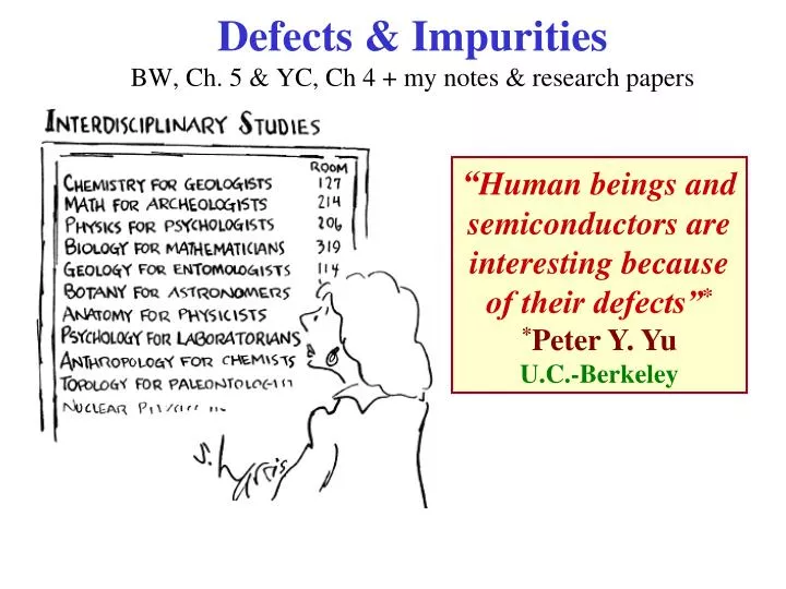
Defects & Impurities BW, Ch. 5 & YC, Ch 4 + my notes & research papers. “ Human beings and semiconductors are interesting because of their defects” * * Peter Y. Yu U.C.-Berkeley. A primary reason that Semiconductors are useful for devices :

E N D
Defects & ImpuritiesBW, Ch. 5 & YC, Ch 4 + my notes & research papers “Human beings and semiconductors are interesting because of their defects”* *Peter Y. Yu U.C.-Berkeley
A primary reason that Semiconductors are useful for devices: The electronic (& other) properties can be significantly altered by incorporating impurities (& other defects) into the material. • There are “good” impurities (& defects) & “bad” ones! Good Impurities: Are useful for device operation. Bad Impurities: Can make devices useless!
Semiconductors, Dielectrics, Metals Carrier Concentration Advantage of Semiconductors:Their electrical properties can be “easily changed” by adding impurities DOPANTS Dielectrics 104 cm 1012cm-3 Semiconductors Disadvantage of Semiconductors:Their electrical properties can be “easily changed” by adding impurities CONTAMINANTS 10-4 cm 1020cm-3 Metals Resistivity
Example: Impurities in Silicon Very useful impurities!! “Shallow” Impurity Levels p-type dopants: B, Al, Ga, Inn-type dopants: P, As, Sb Oxygen, Carbon Benign impurities. Potentially dangerous impurities!! “Deep” Impurity Levels Slowly diffusing & rare metalsLa, Y, Zr, Hf, Ta,... Very dangerous for devices!! “Deep” Impurity Levels Fe, Cu,Ni Cr, Mn, Au,..
Industrial Data(~ 5 years ago): The integrated circuit industry consumes ~> 10,000 tonsof Si per year!! Laboratory Data on Si: 10 mg of Feis sufficient to contaminate this amount of silicon to the level of 1011 cm-3 ~10,000 tons!! ~ 10 mg A Practical Question:With such possibilities of contamination, how can a high purity of Si wafers be maintained in the process of manufacturing of integrated circuits?
Example:Degradation of MOS devices by metal precipitates Local thinning of the oxide Trap-assisted tunneling
Effect of Iron (Fe) Contamination on MOS Devices Threshold Iron Concentration Note:Fe contamination isn’t the only problem! Contamination of Si (& other materials) by most other metal atoms is also very dangerous!!
There are at least two solutionsto the problem of how to keep metal contamination low in semiconductors 1. Ultra-Clean Technology Growth Technology 2. “Defect Engineering” Physics!! Metals are dangerous only if they are in the device-active region. If metals can be removed from the devices, & localized in pre-defined regions of the wafer, or if they can be “passivated”, they will not affect the device yield. However, defects can be “engineered” only if we know a lot about their PHYSICS!!
Ultra-Clean Technology
NOTE! • To alter the electronic properties of a semiconductor only requires a very smallabsolute impurity concentration: (NI/NH) ~ 10-6 (NI =# impurity atoms, NH =# host atoms) • Also, impurities & defects CANproduce energy levels in the fundamental bandgap of the perfect crystal. Controlling the impurity concentration is VITALto device performance! • A first step to controlling them is obtaining a Theoretical understanding of their Physics.
Effect of Various Substitutional Impurities on the Resistivity of Si
Some Measured Impurity Levels in Ge Shallow Donor Levels Shallow Acceptor Levels
Some Measured Impurity Levels in GaAs This shows that the measured energy for an impurity may “depend on the measurement technique”!
Some Measured Shallow Donor Levels in Semiconductors
Defects & Impurities • From the data, impurity & defect levels in semiconductor bandgaps arediverse, varied, & complicated, even for “simple” substitutional impurities! • In addition to impurity levels, there can also be bandgap levels due to complex defects. • It is now known that the bandgap levels can be understood as being “signatures”of defects & impurities. NOTE • Whole books have been written on defects & impurities in semiconductors! • So, we will just discuss the highlights.
Classification of Defects & Impurities Classification by Level Depth • One obvious way to classify impurities & defects is by their level “depth” in the bandgap. “Shallow” Impurities • These produce bandgap levels near the conduction or valence band edges. • These can be accurately calculated by Effective Mass Theory(“Effective Hydrogen Atom Theory”). We will describe this theory in some detail. “Deep” Impurities • All others. We will describe a theory of these in detail.
Classification by Spatial Extent • Another way to classify impurities & defects is by the spatial extent of their potential and their wavefunction. Point Defects • These are isolated atoms or small groups of atoms (complexes). This kind is all that we’ll discuss here. • Point defects can be either good or bad for the material, depending on the individual material and defect. Line Defects • These are defects in which rows or planes of atoms are involved (such as dislocations). These are usually bad for the material. We won’t discuss these here.
Types of Point Defects & Impurities • Vacancy:A missing atom at a lattice site. • The symbol is VA for a missing atom of type A. • Interstitial: An atom in between lattice sites. • It is possible to have a self-interstitial. • The symbol is IA for an atom of type A at an interstitial site. • Substitutional Impurity:An impurity atom C replacing a host atom A. • The symbol is CA for an atom of type C replacing an atom of type A. • Antisite Defect:In compounds only. A host atom B occupying a site that should have had a host atom A on it. • The symbol is BA for an atom of type B on an A site.
Types of Point Defects & Impurities • Complexes:Combinations of some point defects. • For example, a vacancy - interstitial pair: VA-IA Other Classifications • Intrinsic or Native Defects:No matter what the growth process is, these cannot be completely eliminated. • Examples:Vacancies, Antisite Defects, Self-interstitials. • Extrinsic Defects:Impurities or impurity complexes of some sort.
Point Defects & Impurities • Our main interest in this discussion will be Electrically Active Defects • Donors: Contribute electrons to the host material. • Acceptors: Accept electrons from the host. Or donate Holes to the host. • Isoelectronic Impurities: Are substitutional impurities from the same column of the periodic table as the host atom being replaced.
Consider Si (or any column IV atom material) Some Single Donor Impurities: • These are impurities from column V of the periodic table (P, As,…) Some Single Acceptor Impurities: • These are impurities from column III of the periodic table (B, Al, Ga,..) • There are also Double Donors or Double Acceptors, etc. which donate or accept two electrons.