Download

1 / 17
180 likes | 351 Vues
2. Bolometer Technology I 6.1 Pixel Thermal Design. SCUBA-2 Pixel Thermal Design. Can we design a pixel that meets a number of constraints and satisfies certain design criteria? We have constructed a model that allows us to optimise various parameters in an attempt to answer this.

E N D
2 Bolometer Technology I6.1 Pixel Thermal Design
SCUBA-2 Pixel Thermal Design Can we design a pixel that meets a number of constraints and satisfies certain design criteria? We have constructed a model that allows us to optimise various parameters in an attempt to answer this.
What are the constraints to the thermal design? Sensitivity: Phonon NEP must be lower than the background photon noise limit. Time constant: Must be fast enough for fast scanning, but slower than 6L/R for stable operation. Bias power: Have low bias power (current) to minimise noise. Passband: Clean, low noise passband. Pixel structure: A simple structure with good absorption. Ideally the same structure for both arrays. Bias setting: Must be able to cope with high and variable background.
Bias setting constraints > operate on constant point on R-T curve > have
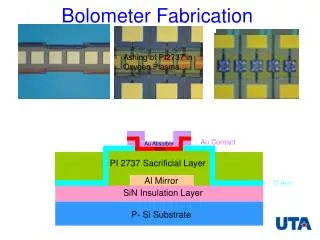
Pixel Structure: Proposed Design 0.5F = 1.135mm, assuming F=2.67, =850m 50m AuPd absorber (~50nm thick) Silicon walls 450m 1.065mm Silicon Layer /4n = 61m at 850μm 1m or less 10m SiN membrane MoCu bilayer TES (200nm thick)
Heat Capacity Estimated contributions of the various materials to the heat capacity at 120 mK If the total heat capacity is dominated by the TES structure
850m pixel model Initial assumptions: Tbath=60mK, L=2H At some transition temperature, Tm,we also have m=50, Rm=25m The background power from the sky will vary between Qmin=7pW and Qmax=18pW Assume a bias power of 5pW (typical value used) The key requirement is to try to keep the TES biased so that it remains at a constant operating point, and the variation in normalized responsivity is < 1% As can be seen in the next plot the bias power is too low to make up difference in background, and so a heater is needed on each pixel.
Example 1: Adopt a thermal conductance, G=2000pW/K and Tm=120mK where P(T) is the total power in the device, Q(T) is the difference between the total power and the bias power. Q(T) is therefore made up of the sum of background and heater power.
Responsivity and time constant variation Time constant is too slow at Tm Cannot lower the bias to say, 118mK, since the bias power is too great G=2000 pW/K Tm=120 mK
Normalised responsivity variation Change in responsivity is too great G=2000 pW/K Tm=120 mK
Noise equivalent power Easily meets the specification G=2000 pW/K Tm=120 mK
In summary: Pixel design does not work at Tm since the responsivity changes too quickly with background power and the device is too slow. Re-biasing to 118 mK to reduce the responsivity variation gives too much bias power and makes the device too fast... Can re-bias but makes it harder to get a stable bolometer against background changes. Try increasing and Tm, and reducing G and bias power =200, Tm=300mK G=1000pW/K, Pbias=3pW at 300mK
Example 2: Adopt a thermal conductance, G=1000pW/K and Tm=300mK T
Responsivity and time constant variation Time constant is still too slow at Tm but can now bias lower, say at 299 mK G=1000 pW/K Tm=300 mK
Normalised responsivity variation Change in responsivity is ~1% at 299mK G=1000 pW/K Tm=300 mK
Noise equivalent power Noise level is higher but still meets the specification G=1000 pW/K Tm=300 mK
Conclusions • Low devices will be difficult to use in stare mode unless they are very uniform. • More design room to bias at bottom of transition by increasing C (reduce TES area and add palladium). • Thermal design is a compromise between noise, speed and stability (and chip heat dissipation). We can control Vbias, C, Tm and G, but what about ? • A heater with an accurate power setting, and a feedback system to keep average bias power constant, is needed (takes out drifts in sky background due to airmass and opacity changes). • Simplified model, but the message is to bias in the bottom of the R-T curve and have a large enough .