Download
1 / 23
290 likes | 738 Vues
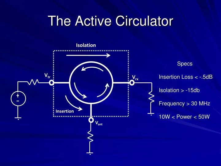
The Active Circulator. Isolation. V tr. V rx. V ant. Insertion. Specs Insertion Loss < -.5dB Isolation > -15db Frequency > 30 MHz 10W < Power < 50W. 3 NPN Circulator. Small Signal Diagram Purpose: Design a CCW circulator out of a 3-port, 3-transitor network.

E N D
The Active Circulator Isolation Vtr Vrx Vant Insertion Specs Insertion Loss < -.5dB Isolation > -15db Frequency > 30 MHz 10W < Power < 50W
3 NPN Circulator Small Signal Diagram Purpose: Design a CCW circulator out of a 3-port, 3-transitor network. Design: Construct h-parameter admittance matrix. Then find transistor parameters that make it behave like a circulator.
Experiment Results Operating Points: Vtrs= 100mV, f = 1kHz Results: Isolation = -19.33dB, Insertion Loss = -1.012dB Power = 1.13mW
Considerations Cons: Bias Current Vbe Overdrive Rpi Sensitivity Pros: High Frequency Parameters Easily Calculated Symmetric
Basic Model Purpose: A more “flexible” op-amp Design Specs: V1=V2=7.5V V3=-0.8V IR1=IR2=1mA
3-Port Scheme • Idea from the topology in the proposal
Continued: Simulation Result Insertion Loss: -1.41DB Need simplification for analysis purpose.
Continued-Small Signal Test Signal From the Transmitter (f_input=1kHz) Vtransmitter=49.60mV Vantenna=25.2mV Vreceiver=1.84mv F(-3db)=298.7kHz Insertion Loss=-6DB Isolation Loss=-31.50DB Signal From the Receiver (f_input=1kHz) Vantenna=49.8mV Vreceiver=43mv Vtransmitter=0mV F(-3db)=805.3kHz Insertion Loss=-1.27DB Isolation Loss=-Inf
Continued Large Signal Test Signal From the Transmitter (f_input=1kHz) The largest input signal before distortion is 11.5V Signal From the Receiver (f_input=1kHz) The largest input signal before distortion is 4.0V Clipping Distortions
Basic Model Purpose: To understand the limiting factors involved with Op-Amps used in this topology 3-Port, Symmetric, Op-Amp Topology Method: Push the limits of readily available LM741 Op-Amps, to better understand the capability of this topology.
Testing Results Small Signal Test: Ro: 11k VBIAS: +/- 20 DC Vtr : 250mVpp Vant(-3dB) occurred at 180 kHz Large Signal Test: Ro: 11k VBIAS: +/- 20 DC Vtr : 17Vpp Vant(-3dB) never occurred, clipping Clipping occurred at 8kHz, yielding calculated slew rate of .427 V/us Isolation: Ideal operating condition, 1 Vpp @ 1 kHz : -23.7 dB Small Signal max frequency: -10.17 dB Large Signal max frequency: -29.19 dB
Alternative Model This model was determined to be too finicky with resistance mismatching. Far too much distortion was found in the experiments, and the topology was abandoned The input was a sinusoid…
Testing Results • Small Signal Test: Ro: 11k VBIAS: +/- 20 DC Vtr : 200mVpp Vant(-3dB) occurred at 224 kHz • Large Signal Test: Ro: 11k VBIAS: +/- 20 DC Vtr : 1Vpp Vant(-3dB) occurred at 200kHz • Dr. Young mentioned frequency should be our focus, not power, • hence, the significantly smaller large signal voltage. • Isolation: Ideal operating condition, 1 Vpp @ 1 kHz : -25.03 dB Small Signal max frequency: -29.05 dB Large Signal max frequency: -49.11 dB
Summary • Pros: Simplest design Specifications easiest realized • Cons: Voltage divider Frequency limited to available Op Amps Heating Issue Phase shift at frequency limits
Conclusion There are many paths we can take. Pursue high power: Op/Diff amp design Pursue high frequency: 3 transistor Pursue a compromise… We recommend the Op/Diff amp design because it is the most realizable.