Download
1 / 10
110 likes | 260 Vues
Read this presentation to know more about semiconductor wafers like Silicon Wafers, FZ Wafers, SOI Wafers. For more information visit www.waferpro.com

E N D
WAFERPRO Best Semiconductor Wafers 410 E Santa Clara St # 518, San Jose, CA, USA 95113
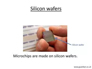
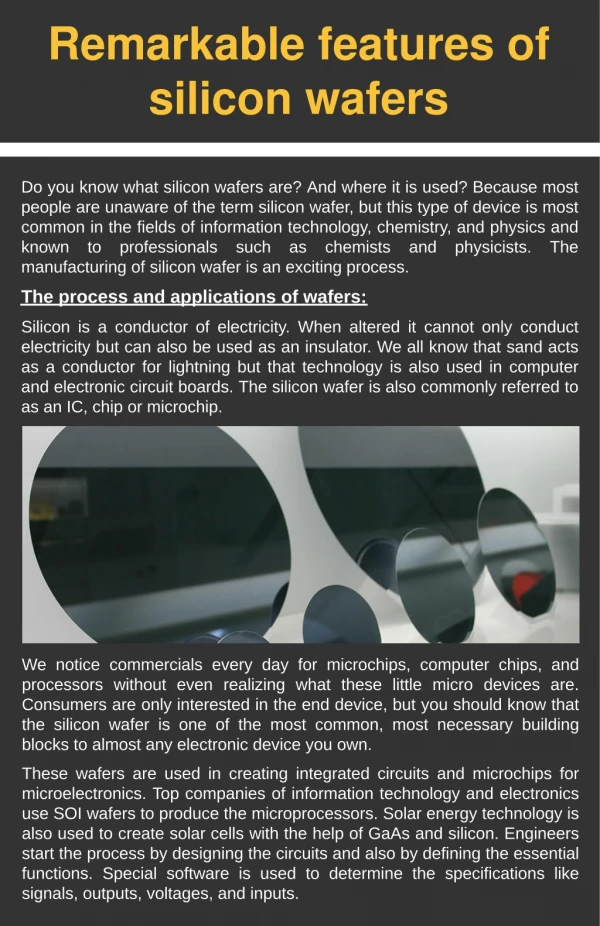
DEFINITION OF WAFER A wafer is a thin single-crystal semiconductor that is used in the manufacture of semi-conductor devices as well as integrated circuits. Depending on the material used, wafer may have diameter ranging from about 25-300 mm. Wafer substrates microelectronic devices that are built over and in the wafer and also do undergo many different micro fabrication process steps like ion or doping implantation, deposition of different materials, photolithographic patterning and etching. The last step of the whole process is the separation of the individual microcircuits and packaging.
FORMATION OF WAFERS The formation of wafers is done by the use very pure single crystal material. The process is done by two methods. The following are the two mainly known methods used to form wafers; - Czochralskigrowth (CZ). This method was invented by Jan Czochralski. During this process, the formation of germanium or silicon is by pulling seed crystal from "melts." - Float-zone crystal growth (FZ). This is a method that is used in the formation of single crystal substrate of semiconductors. It is an alternative to Czochralski growth (CZ). Unlike Czochralski growth, Float zone crystal growth produces the best semiconductor wafers. This explains why it is the commonly used method in the formation of semiconductor wafers.
SILICON WAFERS Silicon is a brittle, tetravalent, gray chemical element. It makes up to 27.B% of the crust of the earth. It is among the most abundant and important elements of nature (next to oxygen). Silicon is an element that can be found in materials like agate, quartz, flint and also common beach sand among many others. In building materials such as bricks, glass and cement, silicon is the main component. Majority of different micro chips and semiconductors are built on silicon. The irony of silicon is that by itself it cannot conduct electricity very well. However, it is be able to take on dopants so as to control resistivity to the exact specification. A transformation of silicon into a wafer must take place before building a semiconductor. The beginning of this is in the growth of the silicon ingot. A silicon crystal is just a solid that is composed of several atoms that are arranged in a periodic pattern that is in three dimensions and that extends throughout the whole material. The formation of a polysilicon crystal is by different single crystals that are small and with orientations that are different. A polysilsicon cannot be considered a semiconductor device alone.
FZ WAFERS PRODUCTS There are many different techniques that are used so as to modify the behavior and characteristics of silicon wafers during their production. Depending on the purpose or project of a silicon wafer, different modification types can be made to the silicon wafer. Float zone wafers are among the many and the best modification types that can be used
WHAT ARE FZ WAFERS PRODUCTS Flat zone wafers are products of wafers that are created through the method of float zone method. Float zone method is based on a principle invented in 1962. It was founded on the principle of zone-melting. Through a necking process and a partial melting, a purified and single crystal is formed. The purity of float zone method makes it possible for the silicon to go through the process of doping which is somehow lighter. The levels of resistivity of wafers that are formed through this method can be very high.
APPLICATIONS OF FZ WAFERS PRODUCTS There so many applications of FZ wafer products. Below are some of them; 1. These silicon wafers are used generally for detector applications and power devices. 2. High efficiency RF chips and solar products is another common application of the float zone wafers. 3. FZ wafers can also have different optical applications. They are typically used in the manufacture of windows and lenses for terahertz applications.
COMPANIES MANUFACTURING FZ WAFERS PRODUCTS The following are the top companies that are well known for the manufacture of silicon wafers; 1. WaferPro -one of the leading suppliers world wide 2. MEMC Electronic Materials- known to be the global pioneer when it comes to wafer technologies 3. Okmetic- best known for processing the best and high quality silicon wafers. 4. PV Crystalox Solar- known for producing multicrystalline silicon ingots and also wafers for solar power use 5. Shin-Etsu Chemical 6. Siltronic 7. Mitsubishi 8. LDK Solar
APPLICATIONS OF FLOAT ZONE WAFERS There are certain uses of float zone wafers that solely work on the usage of these wafers only. Here are some examples: Making of Optical Components: The use of float zone wafers for the making of optical components like tetra hertz exposure window and lenses that are used by the people exposed to tetra hertz radiation is very important. It is the characteristic feature of FZ wafers to be transparent to tetra hertz radiation and it is due to this feature that it proves to be a boon for doctors who use tetra hertz radiation for medicinal purposes. 2. Making of High Volume Production Solar Cells: Another characteristic feature of FZ silicon wafers is that they have twenty-five percent more solar conductivity than any other semiconductor wafer. This makes it an ideal choice for being used in the solar cells since they absorb more heat from the same unit of area than their other counterparts. Although these are more expensive, the amount of solar energy they fetch more than makes up for their cost. The reason behind their being better conductor is the presence of lesser impurities in them. Other uses of FZ wafers include their usage in the photodetectors that sense electromagnetic energy and power semiconductor devices like rectifiers, thyristors and some special type of power transistors that are used mainly for security purposes.
CONTACT US 410 E Santa Clara St # 518, San Jose, CA, USA 95113 sales@waferpro.com (408) 622-9129 www.waferpro.com