Download
1 / 22
220 likes | 290 Vues
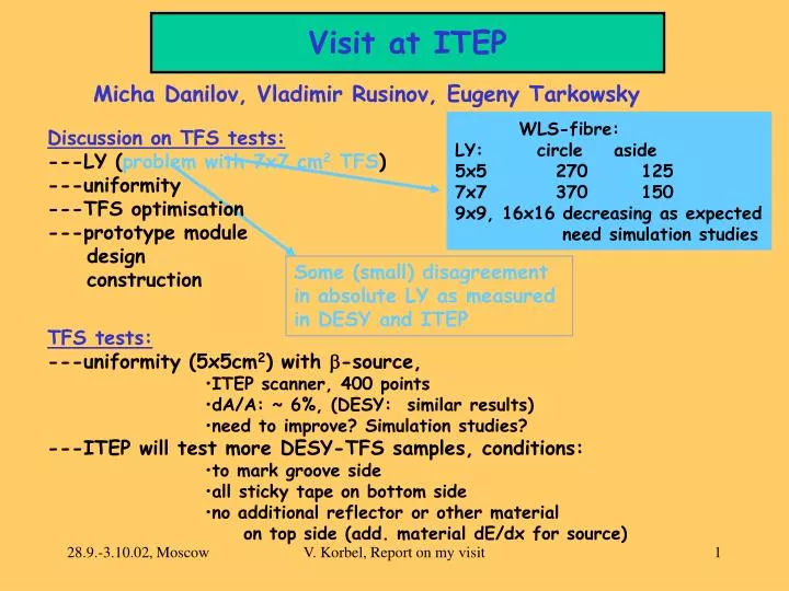
Visit at ITEP. Micha Danilov, Vladimir Rusinov, Eugeny Tarkowsky. WLS-fibre: LY: circle aside 5x5 270 125 7x7 370 150 9x9, 16x16 decreasing as expected need simulation studies. Discussion on TFS tests: ---LY ( problem with 7x7 cm 2 TFS )

E N D
Visit at ITEP Micha Danilov, Vladimir Rusinov, Eugeny Tarkowsky WLS-fibre: LY: circle aside 5x5 270 125 7x7 370 150 9x9, 16x16 decreasing as expected need simulation studies • Discussion on TFS tests: • ---LY (problem with 7x7 cm2 TFS) • ---uniformity • ---TFS optimisation • ---prototype module • design • construction Some (small) disagreement in absolute LY as measured in DESY and ITEP • TFS tests: • ---uniformity (5x5cm2) with b-source, • ITEP scanner, 400 points • dA/A: ~ 6%, (DESY: similar results) • need to improve? Simulation studies? • ---ITEP will test more DESY-TFS samples, conditions: • to mark groove side • all sticky tape on bottom side • no additional reflector or other material • on top side (add. material dE/dx for source) V. Korbel, Report on my visit
Visit at ITEP tiles: cleaning procedure reflector: mating vs. “silver-$” fibres: fibre cutting with TiO2 knife, produce one device for DESY? fibre end in tile side wall covered with small 3M mirror foil, glued to tile hot loop bending (110-120 degree) test LY of Y11(100, 150,200) study again some Bicron fibres? Interest on fibre-fibre fusing, device from DESY >>> ITEP • tile plates: • which sizes to cast? 15x15cm2? • Than machining of the smaller tile profiles, e.g. 9 tiles of 5x5cm2 ? • Impossible to make >38 different tile sizes by casting • re-evaluate the DESY test beam results: • is the ratios correct? • total sum outside hit tile? • Study machined prototype with grooves filled with reflective glue? V. Korbel, Report on my visit
Visit at ITEP • Which scintillator to use? • Small tiles from Russian scintillator? • Homogeneity ok. • Larger tiles show wide dips around fibre position (at loops) • and lower LY. • Optimisation, use: • BASF-136 for small tiles (~70% of total area, ~80% of tiles) • BC-408 or BC-404 for large tiles (~30% of area), 15/38 layers V. Korbel, Report on my visit
Visit at ITEP • Discussion on TFS tests • to do: • DESY: • more 3M reflector to ITEP, • also more Y11 fibres, • some Silver -$ paint for fibre end coating • ITEP: • LY and uniformity for the DESY and Protvino TFS, X-check! • Study optimal doting of WLS: Y11(100)...(300) • Study TFS readout with fixed loop diameter but increasing tile dimensions • (also simulation?) • Silver -$ paint and glued 3M as fibre reflector • fibre end || to tile border, finishing polish for both together • fibre/fibre fused connections, (DESY orders glass tubes) V. Korbel, Report on my visit
Visit at ITEP • Discussion on module construction: • ---split ss absorber plate in 2 parts, e.g.: • 17 mm structure plate • 3 mm TFS support plate, to be inserted in stack structure after assembly • need special rigid inter-connections ? • (grooved rails and special fixing bolts) • ---to improve design of 38 plate prototype next 3 month! • thicker absorber plates towards module end ? • > less tile layers, less scintillator • better granularity with same number of channels? V. Korbel, Report on my visit
Visit at MEPHI • Development of Si-PMs • People involved: • Boris Dolgoshein, Elena Popova, Serge Smirnov (MEPHI), ~5 more people • Sergei N. Klemin, PULSAR enterprise • --signal shape: 1ns slope, 10ns FWHM • --photocathode : • 15% efficiency, • 1x1 mm2 or 2x2 mm2, • 3x3 mm2 to many rejects >> increase of costs • --operation voltage ~ 55 V, • --all signals can be adjusted in amplitude: • by a-source to same gain, • using the very narrow 1,2,3,4 Poisson distributed p.e. peaks. • size of a-signal ~ 1.35 MeV, near to MIP signal ! • and by cosmic MIPs: • for calibration to equal signal amplitude for each tile in a cell. • since cells have different # of tiles: • cell signals have to be adjusted to the optimal range in the ADC V. Korbel, Report on my visit
Visit at MEPHI • Proposed: • to connect single Si-PM’s to each individual tile: >>>> • - ~5000 Si-PM’s for HCAL prototype, • - ~800000 Si-PM’s for TESLA HCAL. • Alternatives: • 1. Connection to each single clear fibre at end of tile-plate: • -optical connector needed to connect optical fibre with Si-PM, • -connector adapted to a Si-PM array with pitch distance ~1.5 mm, • -photodetector mask similar to mask for APD-array? • -to develop such array-connector maskwith holes for fibres, • -each fibre in hole fixed by little droplet of “Sekundenkleber” • -Si-PM photocathode needs mechanical protection from optical-fibre end • by a thin plastic disk probably, • 2. Connection in tile: (see V. Rusinov, ITEP) • -Si-PM inserted in milled groove, 2x2x5 mm3 • -and directly glued to the tile and a short WLS fibre, • -maximum optical LY expected. • -inefficient tile volume: 20/12500 = < 2%o • -nuclear counter effect small, 2 mm thick sensitive layer only • 3. No WLS -fibre at all, direct view of scintillator (studies in ITEP) V. Korbel, Report on my visit
Visit at MEPHI • Signal RO from Si-PM: • see also Vladimir Rusinovs talk • via twisted pair cables, • plus a common ground line for all Si-PM on tile-plate • signal from 50 Ohm to ground, capacitive RO possible? • Such a wire RO is • thinner and easier to arrange than optical RO fibres • less attenuation losses of signal • summing of tile signals to cell signals in electrical adder/shaper, • allows to equalise MIP signals from all tiles in a cell! V. Korbel, Report on my visit
Visit at MEPHI Development in MEPHI and Pulsar: Presented were large integrated multi-layer plates with various Si-PM types on it, several hundreds plate ~ 300mm thick, about 10 multilayers, ~80 subsequent production steps development of waver with appropriate masks, ion inplantations, aluminisation, with polysilicon resistor readout, pixel structure with guard rings for x-talk protection, The multilayer parameters for the production process are defined using special software from ISE (Switzerland) signal development also studied, with SPICE. Production in PULSAR factory, ~900 (300) people, (produce transistors, APD’s, multilayer boards..) optical inspection/selection with scope and special devices to idetify rejects by looking for shorts on final multilayer before cutting out individuals planned are 2000 pixels /mm2, now 600 pixels/mm2 it is possible to produce required quantities for prototype next year! V. Korbel, Report on my visit
Visit at MEPHI • Discussion on our needs: • -- 30 Si-PM’s now, to test in minical • -- 150-200 Si-PM’s March 2003, no additional costs • -- 5000 more Si-PM’s are needed for the prototype • Estimated costs on base of this quantities: • mass production price (5000) is 7 Euro/PM. • for 800 000 Si-PM, price estimate is 2 Euro/PM. • Front end electronic: • preamp/shaper needs no large gain, but shaping! • about 1 (<2) Euro per piece expected • adder/shaper and S&H, investigations have to start soon • need connection with LAL and British DAQ group V. Korbel, Report on my visit
Visit at MEPHI • Information from MEPHI needed soon: • --optimal sensitive ADC range needed: • 1pe > 2mV(50 Ohm)>ADC-channel 15-20 ??? • --gain vs. bias voltage, typical • --noise contribution to MIP peak: • noise rate vs. fraction of MIP threshold • noise rate vs. MIP efficiency • needed for minical studies at DESY: • 1. Testing of 5 pieces at DESY, soon • without external amplification • with simple amplifiers/summers from MEPHI (?) • 2. Testing 30 pieces at DESY up to 1.1.2003 • still with CAMAC-RO • with different tile couplings, • with different fibre connections, • compare performance with MA-PM’s. • To contact: • Orsay/Prague • Minsk/Protvino V. Korbel, Report on my visit
Visit at Uniplast, Vladimir • Experience in Shashlik production for LHC-B, ECAL • ~ 2000 modules, 23 layers, ~25 kg each • cast tiles, 10x10cm2, 64 fibre holes • Polystyrene > BASF-143 popob + ptb • We need: • 1. Better Polystyrene from • Dow-Chemical: STYRON-663, “optical clean” (!) • longer atten. length, price ~ 1.3x • we will order 25 kg for tests • tests with: • 5x5cm2, 10x10cm2 tile sizes, • 4mm tick, existing form used • standard and optical clean PS • LY and uniformity measurement in ITEP • 2. For our production special size molds needed, • max. mold size is 40x40cm2, • pressure to withstand is~ 500atm. • cost/mold ~5000-7000$ • production time for molds: ~ 3 month!! • >>> decision on tilesizes up to end 2002!! Big chemical factory, 207 km north-east from Moscow Example: various tile sizes in a single mold V. Korbel, Report on my visit
Visit at Uniplast, Vladimir Example how to produce our tiles in cast procedure together with grooves: To study uniformity 1 mould only: N tile sizes with same loop dimensions V. Korbel, Report on my visit
Visit at Uniplast, Vladimir We will have about 30 different tile sizes in barrel at present 38, to be redesigned (VK) soon it seems possible to reduce the number of casting forms to 6-8 ? Number of Tiles we need: next year (2003) ~ 200 tiles, march, minical, problem with mould cost ~ 5 000 tiles, autumn, production is some weeks for TESLA HCAL ~ 800 000 tiles, production after 2003, full quantity in 4 years V. Korbel, Report on my visit
To do: • 1. cleaner PS than STYRON-663 (1.3E/k) or 637 (1.3E/kg) • needed for large tile sizes: • >> STYRON-2262 (1.5E/kg) • >> DESY tries to buy, problem delivery outside US ! • 2. produce some new tiles (10x10cm2, directly with grooves) • compare with old PS at ITEP • 3. re-design tile-plate structures (in barrel) • number of tile layers, • define the various tile sizes • exact tile thickness, tolerances ? • 4. final decision on groove shapes (geometrical configuration) • 5. order 1. casting form for HCAL-prototype, • should cover many tile sizes from 5x5 to 8x8cm2, • 6. larger tiles to be machined from cast plates (40x40cm2, Uniplast) • and from BC-408, several m2 more to order? Visit at Uniplast, Vladimir V. Korbel, Report on my visit
Visit at Protvino • With Valentin Kozlov, LPI • New division for plastic production on PS pressure casting base • financial support from government: “new technology support” • use many production parameters, computer controlled • --2 high pressure (~800 kg/cm2) injection machines (DEMAG, new) • --1 extrusion machine (Koch GmbH) • they produce: • commercial products • plastic scintillators • (KOPIO, Phenix,HERA-B, Hermes, many Russian clients) • medical products, clean room set up • Alexander Soldatov • Vladimir Vasilchenko V. Korbel, Report on my visit
Visit at Protvino Scintillator material: PS, Popop, PTB I bought and brought 5 new scintillator cooking ingredients to shift optimally scintillator light to the WLS sensitivity range test are in preparation to improve LY special for Y11-WLS fibre Injection moulding from granulate, max 600 cm2 area or 600 cm3 volume, each casting mould costs ~7000$. to be optimised: mold temperature, pressure, heating/cooling cycles (Protvino+LPI) e.g. 5x5 cm2 tiles: 40 s maximal sizes need: 2-3 min/tile 2 y needed for all TESLA tiles, as a ISTC fund? Total cost ~ 800 000 Euro, 20 E/kg V. Korbel, Report on my visit
Visit at Protvino Discussion on tile arrangement in tile-plates: ---> 4 tile-plate, produced in 1 casting step with ~1 mm connection bridges kept, ~ 2% X-talk expected, up to 20x20 cm2 moulds can be used! Sub-tile plates V. Korbel, Report on my visit
Visit at Protvino Ideas for tile-plate arrangement from individual tiles: 0.7 mm holes V. Korbel, Report on my visit
Visit at Protvino Clamping method, individual. tiles: easier for diagonal curved, much easier for centre grooves Multi tile-plate moulding: not flexible enough for various tile sizes To be discussed: cassettes for tile plates --Support plate needed on both surfaces of tile plate: to carry the tiles (below, 3-5 mm ss?) --to protect the fibres: and make assembly light tight for tests and gain adjustment (on top thin carbon fibre material?) --closing on sides: light tight closing to get light shield and carry the photodetectors (in case of 1 Si-PM/fibre) To fix very soon: --tile sizes, # of tiles per tile size, --grouping of tiles in common moulding forms, --geometrical fibre-groove shapes, --number of casting moulds needed. V. Korbel, Report on my visit
Visit at Protvino • To do: • Protvino: • improve TFS-LY • with new doping ingredients, • with new granulate from DOW Chemical, • try to include fibre grooves in casting, • define # of matrices needed, • produce ca 30 tiles of 5x5 cm2 for minical tests, • work out cost and time plan for HCAL prototype. • ITEP/DESY: • more studies on inserted WLS and clear RO fibre • glue WLS/clear fibre connection, fix on tile • try 1.0 and 1.1 mm clear fibre (to study with LPI?) • fuse WLS/clear fibre connection V. Korbel, Report on my visit
Visit at Protvino • Preamplifiers for use with APD’s • Youri Guilitsski, group of Sergei Denissov: • --ITEP/Minsk type, charge sensitive, • --1 preamp ready • --end Nov.02: some preamps to DESY for minical tests • gain to regulate (by screw driver) up to 5mV/fC • same noise level as from CERN tests • capacity range 20-30 pF • --larger quantity (~ 30 pieces) at 1.1.03 • --PC board with 16 channels (prototype) needs 1/2y production time. • --decision meeting which preamp(s) to choose for prototype • at DESY in Febr.03, Youri comes to DESY V. Korbel, Report on my visit