Download
1 / 6
60 likes | 85 Vues
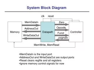
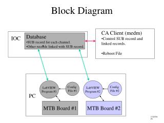
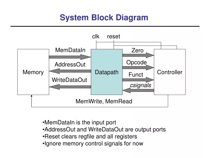
System Block Diagram. clk. reset. MemDataIn. Zero. Memory. Datapath. Controller. Opcode. AddressOut. Funct. WriteDataOut. csignals. MemWrite, MemRead. MemDataIn is the input port AddressOut and WriteDataOut are output ports Reset clears regfile and all registers

E N D
System Block Diagram clk reset MemDataIn Zero Memory Datapath Controller Opcode AddressOut Funct WriteDataOut csignals MemWrite, MemRead • MemDataIn is the input port • AddressOut and WriteDataOut are output ports • Reset clears regfile and all registers • Ignore memory control signals for now
Program Execution • Only two system inputs, reset and clock • Reset zeroes out all registers • Sets PC to first memory address • After reset the program at location 0 should be executed • PC should increment after each instruction (except beq) • Memory must contain program at address 0
Controller Design zero Controller ALU Control aluOP opcode (IR 31-26) funct (IR 5-0) ALU control signals most control signals • Datapath needs new outputs opcode and funct • Controller is sequential, ALU Control is combinational • Reset and clock signals not shown
Main Controller • A big case statement based on the opcode case (opcode) begin 35: cseq_lw(sclk); 43: cseq_sw(sclk); 0: cseq_rtype(sclk); … • Assume a task for each instruction type • Opcodes will be given to you
ALU Control • A big case statement based on ALUOp and funct case (ALUOp) begin 00: ALUcontr = 010; 10: case (funct) begin 32: ALUcontr = 010; … • Assume a task for each instruction type • Opcodes and functs will be given to you
Testing the CPU • Modify the Verilog code of the memory • Write a program starting at location 0 • Reset the machine • Check the results of the program