Download
1 / 17
190 likes | 451 Vues
Microprocessor. Address Decoding. Topics to be discussed ADDRESS DECODING A simple NAND gate decoder Sample Decoder Circuit The Dual 2-to-4 Line Decoder (74LS139) PLD Programmable Decoders. ADDRESS DECODING

E N D
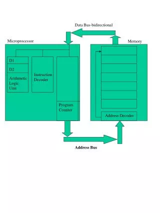
Microprocessor Address Decoding
Topics to be discussed • ADDRESS DECODING • A simple NAND gate decoder • Sample Decoder Circuit • The Dual 2-to-4 Line Decoder (74LS139) • PLD Programmable Decoders
ADDRESS DECODING • In order to attach a memory device to the microprocessor, it is necessary to decodethe address sent from the microprocessor. • Decoding makes the memory function at a unique section or partition of the memory map. • Without an address decoder, only onememory device can be connected to a microprocessor, which would make itvirtually useless. BACK
? • Why Decode Memory • The 8088 has 20 address connections andthe 2716 EPROM has 11 connections. • The 8088 sends out a 20-bit memoryaddress whenever it reads or writes data. • because the 2716 has only 11 address pins,there is a mismatch that must be corrected • The decoder corrects the mismatch by decoding address pins that do not connectto the memory component.
Simple NAND Gate Decoder • When the 2K 8 EPROM is used, address connections A10–A0 of 8088 are connectedto address inputs A10–A0 of the EPROM. • the remaining nine address pins (A19–A11)are connected to a NAND gate decoder • The decoder selects the EPROM from one of the 2K-byte sections of the 1M-byte memory system in the 8088 microprocessor. • In this circuit a NAND gate decodes the memory address, as seen in Figure 10-13. BACK
A simple NAND gate decoder that selects a 2716 EPROM for memory location FF800H–FFFFFH.
If the 20-bit binary address, decoded by the NAND gate, is written so that the leftmost nine bits are 1s and the rightmost 11 bits are don’t cares (X), the actual address range of the EPROM can be determined. • a don’t care is a logic 1 or a logic 0, whicheveris appropriate • Because of the excessive cost of the NAND gate decoder and inverters often required,this option requires an alternate be found.
The 74LS138 3-to-8 line decoder and function table. The 3-to-8 Line Decoder (74LS138) • a common integrated circuit decoder found in many systems is the 74LS138 3-to-8 line decoder.
Sample Decoder Circuit • The outputs of the decoder in Figure 10–15, are connected to eight different 2764 EPROM memory devices. • The decoder selects eight 8K-byte blocks of memory for a total capacity of 64K bytes. • This figure also illustrates the address range of each memory device and the common connections to the memory devices. BACK
connected to this circuit. • the decoder’s outputs are connected to the CE inputs of the EPROMs, • the RD signal from the 8088 is connected to the OE inputs of the EPROMs all address connections from the 8088 are Figure 10–15 A circuit that uses eight 2764 EPROMs for a 64K 8 section of memory in an 8088 microprocessor-based system. The addresses selected in this circuit are F0000H–FFFFFH.
In this circuit, a three-input NAND gate is connected to address bits A19–A17. • When all three address inputs are high, the output of this NAND gate goes low and enables input G2B of the 74LS138. • Input G1 is connected directly to A16. • In order to enable this decoder, the first four address connections (A19–A16) must all be high.
Address inputs C, B, and A connect to microprocessor address pins A15–A13. • These three address inputs determine which output pin goes low and which EPROM is selected whenever 8088 outputs a memory address within this range to the memory system.
The Dual 2-to-4 Line Decoder (74LS139) • Figure 10–16 illustrates both the pin-out and the truth table for the 74LS139 dual 2-to-4line decoder. • 74LS139 contains two separate 2-to-4 line decoders—each with its own address, enable, and output connections. • A more complicated decoder using the 74LS139 decoder appears in Figure 10–17. BACK
Figure 10–17 A sample memory system constructed with a 74HCT139.
PLD Programmable Decoders • Three SPLD (simple PLD) devices function in the same manner but have different names: • PLA (programmable logic array) • PAL (programmable array logic) • GAL (gated array logic) • In existence since the mid-70s, they have appeared in memory system and digital designs since the early 1990s. BACK
PAL and PLA are fuse-programmed, and some PLD devices are erasable devices. • all are arrays of programmable logic elements • Other PLDs available: • CPLDs (complex programmable logic devices) • FPGAs (field programmable gate arrays) • FPICs (field programmable interconnect) • These PLDs are more complex than the SPLDs used more commonly in designinga complete system.