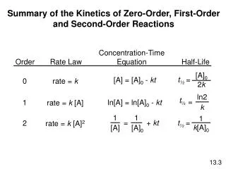
Download
1 / 7
70 likes | 165 Vues
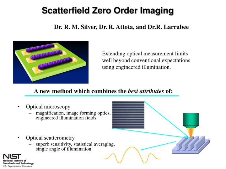
Scatterfield Zero Order Imaging. Dr. R. M. Silver, Dr. R. Attota, and Dr.R. Larrabee. Extending optical measurement limits well beyond conventional expectations using engineered illumination. A new method which combines the best attributes of:. Optical microscopy

E N D
Scatterfield Zero Order Imaging Dr. R. M. Silver, Dr.R. Attota, and Dr.R. Larrabee Extending optical measurement limits well beyond conventional expectations using engineered illumination. A new method which combines the best attributes of: • Optical microscopy • magnification, image forming optics, engineered illumination fields • Optical scatterometry • superb sensitivity, statistical averaging, single angle of illumination
Scatterfield Microscopy • Primary Semiconductor Applications • Critical Dimension (CD) metrology • Overlay metrology • Defect inspection • Nanomanufacturing Applications • Fuel cell process control • Arrayed nanoparticles • Nanometer sensitivity • A technique which enables scatterometry type measurements on very small targets • High throughput, low cost • In chip semiconductor applications • Reduced scribe line target size • Parallel measurements of multiple targets Scatterfield optical imaging: Measuring 10 nm or 20 nm sized features with 450 nm wavelength light. Well beyond conventional resolution limits using engineered illumination and structured targets.
Scatterfield Microscopy • Angle resolved characterization is fundamental to accurate microscopy • Optical system alignment • Polarization characterization • Angular transmissivity • Source characterization • Nanometer scale measurements can be achieved using angle resolved scatterfield microscopy. • Quantitative modeling demonstrated • Nanometer consistency with reference metrology • Dense zero order arrays can be measured • No immediate limitation of feature size or density Scatterfield optical imaging enables the microscope to be characterized in fundamental ways previously inaccessible allowing substantially improved theoretical understanding of optical microscope imaging.
Even illumination at the object focal plane A Field Diaphragm LED Field Lens Condenser A B B C aperture Back focal plane of condenser lens C relay lens objective Tool Configuration: Illuminator Layout Scan axis configuration • 1 cm diameter conjugate back plane for illumination engineering. • Fourier plane engineering on illumination and collection paths. • Can define x and y polarization. • y (parallel) and x (perpendicular) scan axes relative to target lines.
(0,0) Die: Top = 118.6 nmMid = 114.7 nm Bottom = 128.8 nm (0,-1) Die: Top = 116.1 nmMid = 112.3 nm Bottom = 125.1 nm (-1,-1) Die: Top = 102.1 nmMid = 117.0 nm Bottom = 128.9 nm Optical Modeling: Theory to Experiment Agreement Sensitivity: 100 nm CD, Pitch 300 nm Best Fit for 100 nm CD, Pitch 600 nm Plots show intensity as a function of angle. Experimental sensitivity on the left and theory to experiment comparison on the right. These data are an example of zero order imaging with sub-resolution features. • Quantitative agreement obtained for optical modeled measurements. • Optical/AFM agreement on the nanometer scale achieved for the first time.
Overlay/CD Targets: Parallel Measurement Capabilities Line/trench structures 90nm 1:3 Linearity Array Zero order 50 nm CDs • The lines are approximately 60 nm CD +/- 5 nm. • 5 nm changes in linewidth show significant response. • Meets important needs of combined CD and overlay metrology. • In chip metrology capabilities.
Scatterfield Zero Order Imaging Summary: Low cost high, throughput technique with applications in process control and metrology for semiconductor manufacturing and emerging nanotechnology industries. Can measure sub-20 nm sized features, densely positioned with nanometer scale accuracy over very large areas. Patent Application, serial # 11/866,589 filed 11/1/07