Download
1 / 51
1.49k likes | 2.57k Vues
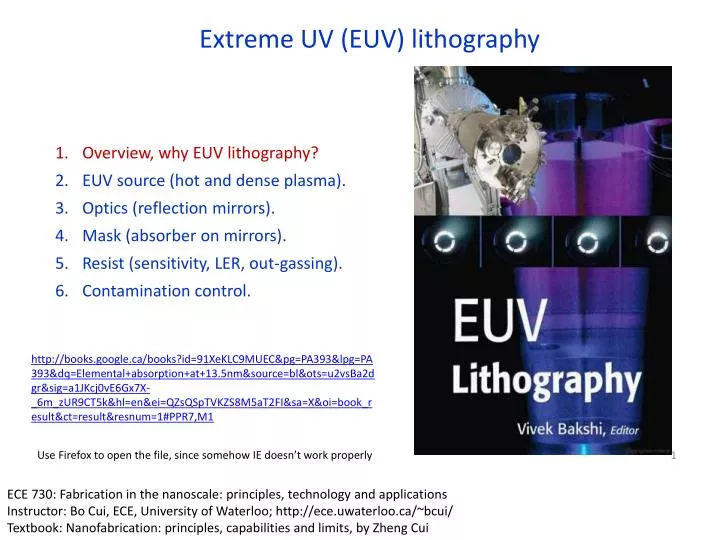
Extreme UV (EUV) lithography. Overview, why EUV lithography? EUV source (hot and dense plasma). Optics (reflection mirrors). Mask (absorber on mirrors). Resist (sensitivity, LER, out-gassing). Contamination control.

E N D
Extreme UV (EUV) lithography • Overview, why EUV lithography? • EUV source (hot and dense plasma). • Optics (reflection mirrors). • Mask (absorber on mirrors). • Resist (sensitivity, LER, out-gassing). • Contamination control. http://books.google.ca/books?id=91XeKLC9MUEC&pg=PA393&lpg=PA393&dq=Elemental+absorption+at+13.5nm&source=bl&ots=u2vsBa2dgr&sig=a1JKcj0vE6Gx7X-_6m_zUR9CT5k&hl=en&ei=QZsQSpTVKZS8M5aT2FI&sa=X&oi=book_result&ct=result&resnum=1#PPR7,M1 Use Firefox to open the file, since somehow IE doesn’t work properly ECE 730: Fabrication in the nanoscale: principles, technology and applications Instructor: Bo Cui, ECE, University of Waterloo; http://ece.uwaterloo.ca/~bcui/ Textbook: Nanofabrication: principles, capabilities and limits, by Zheng Cui
Electromagnetic spectrum • Visible is 400 - 700nm (1.7 to 3eV) • UV down to about 170 nm (7eV) • VUV- Vacuum UV (starts where N2 is absorbing) then there is FUV (far UV) & EUV • EUV/soft x-ray, 2-50nm • 47nm is the λ for the Ne-like-Ar X-ray Laser (capillary discharge laser). • But for EUV lithography, it is at 13.5nm (92eV).
Why EUV lithography? • Shorter gives higher resolution. • No need of resolution enhancement techniques. • Relax the requirement for NA. • For EUV lithography, =13.5nm where efficient “lens” (reflected mirror) exists.
Some history of EUVL (not long) 10 reduction, namely feature size in mask is 10 that of in resist In 1994, EUVL is not considered as a feasible lithography; instead x-ray lithography and e-beam lithography are believed to be the successors to optical lithography. Today, EUVL is regarded the most promising next generation lithography.
Transitions to EUV is a big jump Big jump from 193 to ~13 nm. Before this has about ¼ increase in energy. Now >10x There are only so many “tricks” to increase this gap, and they are very expensive … we must go to a shorter wavelength! Mask Maker’s Holiday: “large” k1 Mask Maker’s Burden: “small” k1 In 2004, it is predicted that EUVL will become mass production tool in 2009. Today it is believed that DUV lithography (=193nm) with double processing will be used for 32nm generation production, thus delaying the need for EUV.
Reticle (Mask) Wafer 193 nm Excimer Laser Source Exposure Column (Lens) Computer Console Why not the next excimer line? • Current 193nm DUV lithography • Lenses are very effective and perfectly transparent for 193nm and above, so many are used: a single “lens” may be up to 60 fused silica surfaces. • System maintained at atmospheric pressure. • Exposure field 26x32mm2. • Steppers capable of exposing 109 steps per 300mm wafer, and produce >100 wafers per hour. Exposure times 10-20ns (one pulse of excimer laser). www.tnlc.ncsu.edu/information/ceremony/lithography.ppt
Current 193nm deep UV (DUV) lithography: mask material • Photo-masks today are made from fused silica. • Fused silica has a number of advantageous properties. • Chemical stability. • Transparency for ultraviolet light. • No intrinsic birefringence. • A low coefficient of thermal expansion. • A low coefficient of thermal expansion: 0.5ppm/oC. • If a mask changes temperature by 0.1oC, then the distance between two features separated by 50mm will change by 2.5 nm. • This change in registration can be absorbed into overlay budgets, after reduction by 4× (i.e. pattern on resist misaligns by 2.5/4=0.6nm, OK).
Why not the next excimer line (157nm) or 46nm? • Why not a stop at 157nm? • Fused silica and atmospheric oxygen become absorptive by 157nm, so even incremental decreases in wavelength (by only 36nm) start to require a major system modification: vacuum exposure, use CaF2 as lens material. • The coefficient of thermal expansion of CaF2 is 19ppm/oC, versus 0.5ppm/oC for fused silica. • The 2.5nm of mask registration error now becomes nearly 100 nm (25nm after ¼ reduction, still too high). • Below 157nm, no excimer laser line has the required output power. • Why not a stop at 46nm? • Ne-like-Ar X-ray Laser (capillary discharge laser developed at CSU) produces EUV at this wavelength. • The wavelength is >3 longer than 13.5nm, so lower resolution. • Still need reflectance optics, but hard to get high reflectance. • Materials and thicknesses issues (high absorption).
EUV lithography characteristics • EUV radiation is strongly absorbed in virtually all materials, even gases, so EUV imaging must be carried out in a near vacuum. • There is no refractive lenses usable - EUVL imaging systems are entirely reflective. • But EUV reflectivity of individual materials at near-normal incidence is very low, so distributed Bragg reflectors (period about λ/2) are used. • The best of these function in the region between 11 and 14nm (Si/Mo material) • EUV absorption in standard optical photo-resists is very high (low penetration depth into resist), so new resist and processing techniques will be required
Schematic of EUV lithography system EUVL alpha-tool
A few optical designs (using reflective lens/mask) Synchrotron radiation A four-mirror system, holes in M4 to let light pass through. An early simple two-mirror system A six-mirror system having NA 0.25
Extreme UV (EUV) lithography • Overview, why EUV lithography? • EUV source (hot and dense plasma). • Optics (reflection mirrors). • Mask (absorber on mirrors). • Resist (sensitivity, LER, out-gassing). • Contamination control.
plasma target EUV @13.5nm plasma radiation source Light sources must match the wavelengths at which Mo/Si multi-layers have high reflectivity. • The only viable source for 13.5nm photons is a hot and dense plasma • Powerful plasma: temperature of up to 200,000oC, atoms ionized up to +20 state. • Emit photons by (e - ion) recombination and de-excitation of the ions. • Plasma must be pulsed: pulse length in pico- to nanosecond range • Plasma is produced by powerful pulsed laser or electric arc (discharge) of up to 60,000A peak current. Discharge Produced Plasma (DPP) Laser Produced Plasma (LPP) (or Sn vapor) laser pulse (ns) laser 100m
Laser (LPP) and discharge (DPP) produced plasma • DPP: change electrical energy directly into EUV light, so high power, high efficiency; but ablation of electrode and more debris. • LPP: higher collection efficiency (larger collection angle), high repetition rate (more pulses/sec), more manageable thermal loads and debris, more scalable to HVM (high volume manufacturing). • EUV lithography tools using both DPP and LPP have been built. • Challenges: • Radiate from IR to x-ray: need filter. • Large source size into 4π spherical angles: • need collector optics. • Debris and thermal issues: may damage the optics. • For EUV lithography, ideally: • Power > 110W • Maximum in-band emission with narrow bandwidth (≤ ±2%). • Forward directed, no collector • Low (W) to mid-power (1W) has application in other fields: • Interference lithography, spectroscopy, microscopy, other metrology, testing EUV resist.
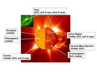
Hot and dense plasma system: the sun EUV Image of the Solar Corona showing loops near the solar limb The loop is due to the magnetic field that bends the electrons/ions http://vestige.Imsal.com/TRACE
Discharge produced plasma (DPP) • Hot plasma is created by magnetic compression of low-temperature plasma. • Plasma is compressed with the magnetic field generated by the current used to heat the plasma, with two common geometries (see figure below). • Because plasma is compressed by magnetic field B of current I, which generates the plasma, plasma is “self-heating”. • Two forces are present: the magnetic field pressure B2/2o and the plasma pressure. • When these two forces are equal, the plasma achieves an equilibrium. Equilibrium: I: total current (BI), supplied by a capacitor in a pulsed mode; Te: electron temperature Ni=r2ni, ni=ion density; Zeff: mean charge of the ions. Two plasma compression geometries.
Laser produced plasma (LPP): overview • LPP is generated by focusing a laser beam on a target material. • Initial ionization occurs through photo-ionization, and the electric field of the laser accelerates these electrons (inverse Bremsstrahlung, see next slides). • Non-elastic collision further ionize the plasma, whereas elastic collision transfers the electron’s kinetic energy into ionic kinetic energy. • As plasma expands, thermal energy is converted into kinetic energy and charge density decreases. (Expansion velocity of Sn plasma at 30eV is about 2106cm/s, so order 100m in front of target for 10ns pulse.) • This decreases both the further absorption of laser energy and energy conversion efficiency (CE). • Therefore, the laser pulse length should not be very long: 10ns is a good time scale. • The corresponding optimum laser intensity for maximum CE is 11011W/cm2 for Nd:YAG laser (1.06m), and 11010W/cm2 for CO2 laser (10.6m). • Modeling shows that CE depends on laser wavelength -- CE (10.6m laser):CE (1.06m laser):CE(0.26m laser)=1.9:1.0:0.55. • This is because: CE depends on a balance between emissivity and opacity; at longer wavelength laser absorption occurs at lower plasma (electron) density that is more transparent for EUV to escape.
Laser produced plasma: a clean, bright, narrow source • Plasma temperature: • Te Z1/5 (2)3/5. Longer wavelength is more efficient to heat up plasma, so higher CE. • : laser wavelength; : laser flux (Watt/cm2); Z: target atomic number. • Energy levels: • Transitions and energy levels are calculated using Hartree-Fock methods. The UTA continuum spectra is due to 4p64dn – 4p54dn+1 + 4dn-14f line transitions. • Atomic processes (routes for radiation): • Ionisation and recombination between successive ion stages. • UTA line radiation from bound-bound transitions (excitation and de-excitation). • Continuous Bremsstrahlung occur as well (Bremsstrahlung: electron emits photon when it is accelerated by the positively charged ions). Same idea as synchrotron radiation where electrons are accelerated radially by magnetic field. From: Soft x-rays and extreme ultraviolet radiation, written by David Attwood
Energy conversion efficiency (CE) into 13.5nm radiation Sn is most efficient, followed by Li (?), then Xe.
Plasma radiation source for 13.5nm: Xe 10.8nm 13.5nm • 13.5nm photons only generated by one ion state (Xe11+). • Maximum population of this state is 45%. • Even this state emits 10 times more at 10.8nm than 13.5nm. • That is, xenon is inefficient: to produce 100W at 13.5nm, kilowatts of other wavelengths would have to be removed. • On the plus side, xenon is very clean and easy to work with (no debris).
Plasma radiation source for 13.5nm: Sn Peak wavelength emission decreased with increasing atomic number ( 1/Z). UTA peak wavelength (nm) versus atomic number Laser produced Sn plasma Target, Z=50 [Kr]5s24d105p2Sn Laser wavelength, 1.064m Laser flux, 1 x 10¹¹ W/cm2 Electron temperature, Te48.8eV Electron density, ne 9.88 x 1020 cm-3 (300K is 26meV, 1eV is 1.15104K) Ion distribution Sn X 0.046 Sn XI 0.243 Sn XII 0.306 Sn XIII 0.330 Sn XIV 0.068 UTA: unresolved transition array, consisting of tens of thousands of lines (unresolved, overlapping 4d–4f transitions).
Sn+8 Sn+7 Sn+6 Plasma compositions for 13.5nm: Tin • Optimum emission when tin is a low-percentage impurity. • Light comes from transitions between 4p64dn and 4p54dn+1 or 4dn-1(4f,5p). • All ion states from Sn8+ to Sn13+ can contribute. • Lighting up these transitions, and only these transitions requires exquisite control of laser plasma. • But tin (debris) tends to condense on optics. • In summary, tin is great as a 13.5nm source, if one can control the debris (yes).
Tin targets from General Atomics Low density (diluted) targets leads to narrow UTA Radiation spectrum 0.5% 100% 0.1% • 100 mg/cc RF foam • 0.1-1% solid density Sn • e.g., 0.5%Sn = Sn1.8O17.2C27H54 1% CE: (energy) conversion efficiency • Low density tin also reduces debris contamination to optics. • The optical depth at 13.5 nm is only ~7 nm of full density Sn. Beyond that, light is reabsorbed. • CE (conversion efficiency) slightly reduced with low density Sn.
Extreme UV (EUV) lithography • Overview, why EUV lithography? • EUV source (hot and dense plasma). • Optics (reflection mirrors). • Mask (absorber on mirrors). • Resist (sensitivity, LER, out-gassing). • Contamination control.
Optics for EUV lithography (EUVL): overview • All solids, liquids, and gasses absorb 13.5nm photons, so no longer refracting lens. • A beam of EUV light is absorbed in 100nm of H2O. • Even worse, conventional optical devices will not reflect EUV light. • EUVL uses concave and convex mirrors coated with multiple layers of molybdenum and silicon -- this coating can reflect nearly 70 percent of EUV light at 13.5nm. • The other 30 percent is absorbed by the mirror. • Without the coating, light would be almost totally absorbed before reaching the wafer. • The mirror surfaces have to be nearly perfect - even small defects in coatings can destroy the shape of the optics and distort the printed pattern in resist. If the thicknesses and compositions of all films are carefully controlled, the reflected light will constructively interfere resulting in the brightest possible reflection. Multiple reflections
Why Si/Mo and 13.5nm? Absorption in solids for EUV and soft x-rays For high reflection, the absorption should be low (i.e. attenuation length should be large). So Mo, Si, Be are good candidates at 10-15nm. • Mo/Si 40 layer pairs ~70% reflectance where Mo and Si are most transparent. • Mo/Be is higher (at =11nm) but narrower; and more importantly, Be is toxic. • Multi-layer coating is more difficult to control for shorter wavelength. Till now mirror for =4.7nm has been fabricated, though less reflectivity and narrower bandwidth.
Refractive index at EUV n=1--i (, <<1), n is close to 1, so low reflection Si3N4 PMMA • Refractive index is closer to 1.0 for shorter wavelength. So no “optics” for x-ray. • For =13.5nm, photon energy = 92eV, so , is not negligible, making reflective optics possible. • Amplitude reflection r=(n1-n2)/(n1+n2) for normal incidence at each interface. http://www-cxro.lbl.gov/, lots of information there
Multilayer EUV mirrors – Bragg reflectors (for normal incidence) m=1, 2… Amplitude reflection r=(n1-n2)/(n1+n2) for normal incidence at each interface. • The mirror is aspheric • For normal incidence, if DA DB, then each layer 3.4nm for =13.5nm. • Since the angle of incidence changes across the mirror, so do the required Mo/Si layer thicknesses. • Acceptable surface roughness: 0.2nm RMS, corresponding to a phase shift error of 10o.
Fabrication and measurement of aspheric mirror Interference fringe pattern • Mirror accuracy sub-1nm globally, GREAT engineering achievement. • Analyze the interference fringe, compare it pixel-by-pixel with the calculated interference fringe pattern for an ideal perfect mirror. • Analyzing the Fourier transformed pattern rather than the wave front directly gives improved accuracy.
Extreme UV (EUV) lithography • Overview, why EUV lithography? • EUV source (hot and dense plasma). • Optics (reflection mirrors). • Mask (absorber on mirrors). • Resist (sensitivity, LER, out-gassing). • Contamination control.
Mask for EUV lithography There can be a capping layer (11nm Si) above the multilayer, to protect the multilayer during the following mask-making processes. (TiO2 doped SiO2 amorphous glass from Corning) Typical thickness
EUV mask fabrication: pattern by e-beam lithography (by DC magnetron sputtering) (use ICP RIE Cl2 gas) (use ICP RIE Cl2/O2 gas) Defects easy to print into resist, so NO defect is allowed in a completed mask. Many defects can be repaired by local heating, focused ion beam milling….
Extreme UV (EUV) lithography • Overview, why EUV lithography? • EUV source (hot and dense plasma). • Optics (reflection mirrors). • Mask (absorber on mirrors). • Resist (sensitivity, LER, out-gassing). • Contamination control.
Resist for EUV lithography • Resist requirements: • High Sensitivity (so allowing weak sources) • High resolution (for small feature sizes) • Low LER (line edge roughness) • Minimal out-gassing (contaminate optics) • Most conventional resists are patternable at EUV. (32nm?) • Absorbance in EUV • The EUV absorbance in organic materials occurs by inner-shell electrons and is therefore - differently from optical lithography - independent of molecular structure. • The absorption of molecules is then equal to the sum of the atomic absorptions. • The strongest absorbing atoms in resists and PAGs are F > O >> N > C, Cl, S, H. (m-1) (PAG: photo-generated acid, for chemically amplified resist)
PMMA has highest resolution, but too slow (low sensitivity) CA: chemically amplified L/S: line/space PMMA C5H8O2 Another issue for PMMA and most other resists is the low penetration depth (order 100nm, need 200nm) into resist at 13.5nm(92eV). So might (or not) need a bi-layer resist process (top for lithography, bottom layer for pattern transfer). Attenuation length (m) Photo-electron absorption edge for inner shell (K, L, M…)
Resist LER (line edge roughness) • LER is due to: • Shot (statistical) noise. At EUV, photons have high energy, therefore low counts and high LER due to statistical photon number fluctuation. • Shot noise needs to be compromised with resist sensitivity. High sensitivity (fewer photons per exposure) leads to high shot noise. Roughly LER(dose)-1/2. • Uncontrolled diffusion of photo-acid (also limit resolution). • Scattering of secondary electrons in resist and substrate (leads to image blur). For 32nm node, need Sensitivity: 2-5mJ/cm2 LER: 1.5nm 2mJ/cm21.36 photon/nm2(!!)
Extreme UV (EUV) lithography • Overview, why EUV lithography? • EUV source (hot and dense plasma). • Optics (reflection mirrors). • Mask (absorber on mirrors). • Resist (sensitivity, LER, out-gassing). • Contamination control.
Contamination and damage to EUV optics • Debris with low velocity will deposit to the mirrors, causing contamination. (debris for Sn or Li source, not for Xe gas source) • Debris with high velocity could damage the optics by sputtering material off the lenses. • Many methods have been tried to manage high energy debris particles: • Gas stopping • Magnetic stopping • Gas plus magnet • Contamination of lens (due to resist out-gassing…): EUV irradiation leads to photochemical reactions that cause hydrocarbons to adsorb to the mirror and mask, reducing mirror’s reflectivity. • Contamination removal methods includes: • UV (>185nm) irradiation in ozone atmosphere at 150oC. • Synchrotron radiation. • DUV (deep UV, =172nm) radiation (simple and efficient).
Gas stops ions, but also stops EUV photons Ion yield at 10˚, 15 cm Faraday cup vs. SRIM estimate Conversion efficiency (CE) at 45˚, 78 cm E-monvs. attenuation calculation Calculated (T: transmission) For instance, for He gas at 100mTorr, 80% ions are stopped at 15cm from source, with CE dropped from 2% to 1.6% at 78cm from source.
Magnetic diversion is partially effective, but not sufficient Magnetic field deflects the movingcharged ions and clusters (debris), with no effect to photons. Force on charge=qv B (q: charge, v: velocity, B: magnetic field) 5 GW/cm2 aluminum free expansion velocityv=6x106 cm/s
Magnetic field plus background gas is most efficient Faraday cup time-of-flight measurements at 10˚, 15 cm from target Photo-ionization peak appears when gas is present No B, no He (100% dense) With B, no He No B, with He With B and He Magnetic field alone (no He) effectively delays the arrival of ions/debris without stopping them.
Hydrocarbon contamination removal by 172nm excimer DUV (deep UV) lamp • DUV at this short wavelength produces oxygen radicals directly from molecular O2, which react with oxygen gas to form ozone. The reactive ozone & DUV oxidize contaminants and they evaporate. • (Longer wavelength, e.g. 185nm, won’t work)
EUVL alpha demo systems and results As of 2007, two alpha demo tools are at research centers