Download
1 / 10
140 likes | 432 Vues
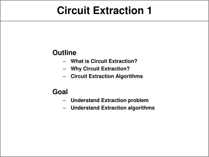
Outline What is Circuit Extraction? Why Circuit Extraction? Circuit Extraction Algorithms Goal Understand Extraction problem Understand Extraction algorithms. Circuit Extraction 1. Convert layout geometry to circuit netlist devices sometimes convert to gates connectivity parasitics

E N D
Outline What is Circuit Extraction? Why Circuit Extraction? Circuit Extraction Algorithms Goal Understand Extraction problem Understand Extraction algorithms Circuit Extraction 1
Convert layout geometry to circuit netlist devices sometimes convert to gates connectivity parasitics Goal verify that layout matches circuit assume layout passes DRC determine actual circuit parasitics back-annotate and resimulate use minimum CPU time, memory integrated extractor + layout editor use existing data structures extract interactively 4/2 4/2 What is Circuit Extraction?
A very crude simulation of manufacturing process how will layout turn into circuit Performance estimated parasitics during design phase compute more exactly with extraction back annotate resimulate and verify circuit still performs as desired Correctness input to DRC, ERC, IV DRC needs some electrical knowledge check that parasitics do not cause electrical rules violation compare designed versus extracted circuit Why Circuit Extraction?
Polygon rectangles as special case most natural representation simple specification of most design rules requires good polygon package Raster at design rule resolution memory hog Tile corner-stitched rectangles, trapezoids good for incremental analysis local connections already stored Edge requires connectivity information minimal memory Geometry Representation 00 10 00 01 11 01 00 10 00
Identify designed circuit elements transistors capacitors resistors inductors Trace connectivity between elements Compute wiring parasitics optional Convert transistors to logic optional Output in suitable format SPICE, EXT, SIM, EDIF,... Extraction Algorithms
Apply boolean operations mask combinations that make different electrical structures use same methods as in design rule checking Examples n_channel = poly active nselect ~nwell p_channel = poly active pselect nwell capacitor = poly electrode Issues identification of passive elements difficult without special layers look just like parasitic elements without pattern recognition region connectivity required for bipolar devices not strictly a lateral or vertical device C E1 B E2 Circuit Element Identification
Find all electrically-connected groups of geometry polygons on same layer that touch are connected identify contacts - both layers in contact are connected Trace net connections corner-stitching - trace in net order by following stitches, contacts bin-sorted polygons - find touching neighbors, follow them A and B touch if A B is one contour contact if top and bottom layers overlap via polygon scan line sweep - build nets as they intersect scan line may need to coalesce nets N1 N2 N1-2 Connectivity
Parasitics of interconnect and devices resistance, inductance, capacitance Range of computation local rules parallel plate, fringing, coupling capacitance contact resistance pattern recognition parasitics of mask configurations e.g. wire crossovers numerical simulation 3-D simulation of structure really accurate, really expensive Parasitic Computation N1, N2, N3 resistance N1, N2, N3 capacitance to substate N1-N2, N1-N3, N2-N3 coupling capacitance N1 N2 N3
Map transistor structures to gates pattern recognition rules technology and design style dependent map into standard cells if standard cell layout can then feed into logic simulation Issues mapping of array structures - PLAs, ROMs, RAMs hierarchical extraction simplifies task often do not extract automatically-generated arrays Logic Identification 3 2 5 5 4 2 4
Extract each unique area once Interaction issue circuit elements usually forbid device creation via cell interaction each cell must be a legal circuit connections - wire crossing cell can connect to it parasitics - capacitance between wires in neighboring cells Issues circuit simulators ultimately need flat circuit hierarchical extraction slower than flat without substantial layout restrictions C12 A.1 B.2 C.5 A B N1 N2 Hierarchical Circuit Extraction