Download
1 / 18
190 likes | 354 Vues
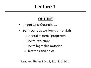
Lecture 1. OUTLINE Semiconductor Fundamentals General material properties Crystal structure Crystallographic notation Electrons and holes Reading : Pierret 1.1-1.2, 2.1; Hu 1.1-1.2 . What is a Semiconductor?. Low resistivity => “conductor” High resistivity => “insulator”

E N D
Lecture 1 OUTLINE • Semiconductor Fundamentals • General material properties • Crystal structure • Crystallographic notation • Electrons and holes Reading: Pierret 1.1-1.2, 2.1; Hu 1.1-1.2
What is a Semiconductor? • Low resistivity => “conductor” • High resistivity => “insulator” • Intermediate resistivity => “semiconductor” • conductivity lies between that of conductors and insulators • generally crystalline in structure for IC devices • In recent years, however, non-crystalline semiconductors have become commercially very important polycrystalline amorphous crystalline EE130/230M Spring 2013 Lecture 1, Slide 2
Semiconductor Materials Elemental: Compound: Alloy: EE130/230M Spring 2013 Lecture 1, Slide 3
From Hydrogen to Silicon EE130/230M Spring 2013 Lecture 1, Slide 4
The Silicon Atom • 14 electrons occupying the first 3 energy levels: • 1s, 2s, 2p orbitals filled by 10 electrons • 3s, 3p orbitals filled by 4 electrons To minimize the overall energy, the 3s and 3p orbitals hybridize to form 4 tetrahedral 3sp orbitals Each has one electron and is capable of forming a bond with a neighboring atom EE130/230M Spring 2013 Lecture 1, Slide 5
The Si Crystal • Each Si atom has 4 nearest neighbors • “diamond cubic” lattice • lattice constant = 5.431Å EE130/230M Spring 2013 Lecture 1, Slide 6
How Many Silicon Atoms per cm3? • Total number of atoms within a unit cell: • Number of atoms completely inside cell: • Number of corner atoms (1/8 inside cell): • Number of atoms on the faces (1/2 inside cell): • Cell volume: (0.543 nm)3 • Density of silicon atoms: EE130/230M Spring 2013 Lecture 1, Slide 7
Compound Semiconductors • “zincblende” structure • III-V compound semiconductors: GaAs, GaP, GaN, etc. • important for optoelectronics and high-speed ICs EE130/230M Spring 2013 Lecture 1, Slide 8
Crystallographic Notation Miller Indices: h: inverse x-intercept of plane k: inverse y-intercept of plane l: inverse z-intercept of plane (Intercept values are in multiples of the lattice constant; h, k and l are reduced to 3 integers having the same ratio.) EE130/230M Spring 2013 Lecture 1, Slide 9
Silicon wafers are usually cut along a {100} plane with a flat or notch to orient the wafer during IC fabrication: Crystallographic Planes and Si Wafers EE130/230M Spring 2013 Lecture 1, Slide 10
Unit cell: View in <111> direction View in <100> direction View in <110> direction Crystallographic Planes in Si EE130/230M Spring 2013 Lecture 1, Slide 11
Electronic Properties of Si • Silicon is a semiconductor material. • Pure Si has relatively high electrical resistivity at room temp. • There are 2 types of mobile charge-carriers in Si: • Conduction electronsare negatively charged • Holesare positively charged • The concentration (#/cm3) of conduction electrons & holes in a semiconductor can be changed: • by changing the temperature • by adding special impurity atoms ( dopants ) • by applying an electric field • by irradiation EE130/230M Spring 2013 Lecture 1, Slide 12
Si Si Si Si Si Si Si Si Si Electrons and Holes (Bond Model) 2-D representation of Si lattice: When an electron breaks loose and becomes a conduction electron, a hole is also created. EE130/230M Spring 2013 Lecture 1, Slide 13
What is a Hole? • Mobile positive charge associated with a half-filled covalent bond • Can be considered as positively charged mobile particle in the semiconductor • Fluid analogy: EE130/230M Spring 2013 Lecture 1, Slide 14
The Hole as a Positive Mobile Charge EE130/230M Spring 2013 Lecture 1, Slide 15
Intrinsic Carrier Concentration, ni • At temperatures > 0 K, some electrons will be freed from covalent bonds, resulting in electron-hole pairs. conduction For Si: ni 1010 cm-3 at room temperature EE130/230M Spring 2013 Lecture 1, Slide 16
Definition of Terms n ≡ number of electrons/cm3 p ≡ number of holes/cm3 ni≡ intrinsic carrier concentration In a pure semiconductor, n = p = ni EE130/230M Spring 2013 Lecture 1, Slide 17
Summary • Crystalline Si: • 4 valence electrons per atom • diamond lattice (each atom has 4 nearest neighbors) • atomic density = 5 x 10²² atoms/cm3 • intrinsic carrier concentration ni = 1010 cm-3 • Miller indices are used to designate planes and directions within a crystalline lattice • In a pure Si crystal, conduction electrons and holes are formed in pairs. • Holes can be considered as positively charged mobile particles. • Both holes and electrons can conduct current. EE130/230M Spring 2013 Lecture 1, Slide 18