Download
1 / 10
120 likes | 230 Vues
Four Channel Portable Electronics. Rubén Conde *, Humberto Salazar*, Oscar Martínez* and L. Villaseñor ** * Facultad de Ciencias FisicoMatematicas, BUAP, Puebla ** Institute of Physics and Mathematics, University of Michoacan, Morelia. HAWC Collaboration Meeting Guadalajara, Méx.

E N D
Four Channel Portable Electronics Rubén Conde*, Humberto Salazar*, Oscar Martínez* and L. Villaseñor ** * Facultad de Ciencias FisicoMatematicas, BUAP, Puebla ** Institute of Physics and Mathematics, University of Michoacan, Morelia HAWC Collaboration Meeting Guadalajara, Méx. Oct 11, 2010
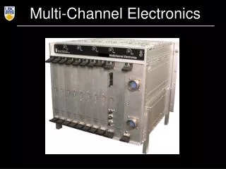
This portable electronics contains A main board Nexys2 (http://www.digitleninc.com) The Nexys-2 is a powerful digital system design platform built around a Xilinx Spartan 3E FPGA. With 16Mbytes of fast SDRAM and 16Mbytes of Flash ROM, the Nexys-2 is ideally suited to embedded processors like Xilinx's 32-bit RISC Microblaze™. The on-board high-speed USB2 port, together with a collection of I/O devices, data ports, and expansion connectors. A daughter board The daughter boad has 4 Channels – 100MSPS 10Bits ADCs dual AD9216 (http://www.analog.com ) The AD9216 is a dual, 3 V, 10-bit, 65/80/105 MSPS analog-to-digital converter. It features dual high performance sample and hold amplifiers and an integrated voltage reference. Input type is single ended and the DC offset of the input signal can be adjusted by means of a programmable 10Bits DAC
Top Diagram(daughter board ) Block ADC Channel 1 and 2 Connector Hirose-FX2 100P To Nexys2 Block ADC Channel 3 and 4
Block ADC Increase Offset for A and B Adder-Inverter A AD9216-100MSPS Dual Adder-Inverter B
Adder-Inverter Connector LEMO
Bottom VIEW JTAG Hirose FX2-100 FPGA Serial Port Top VIEW PCB daughter
Applications four independent channels until 100MSPS use it like two channels of 200MSPS use it like a channel of 400MSPS All this with control of independent level of offset in each channel
Conclusions DAQ System is in test phase -4 Channels until 100MSPS -2Channels unttil 200 MSPS -1 Channel under 400 MSPS Programs for measurements of rate, trace and fix the offset has been developed. GPS & Pressure sensor can be added.
Goal Our proposal is to develop portable DAQ system reliable, low cost and low power consumption that allows to register parameters as the trace, rate and the charge for each signal, among others.