Download
1 / 16
160 likes | 171 Vues
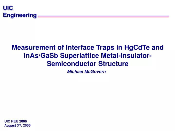
Measurement of Interface Traps in HgCdTe and InAs/GaSb Superlattice Metal-Insulator-Semiconductor Structure. Michael McGovern. UIC REU 2006 August 3 rd , 2006. Applications. Electronics. Astronomy. Security. Medicine. p-i-n Photodiode.

E N D
Measurement of Interface Traps in HgCdTe and InAs/GaSb Superlattice Metal-Insulator-Semiconductor Structure Michael McGovern UIC REU 2006 August 3rd, 2006
Applications Electronics Astronomy Security Medicine
p-i-n Photodiode • Current consists of the flow of “conduction band” electrons and “valence band holes” • The p-i-n photodiode has 3 layers: mostly holes (p), mostly electrons (n) and a region of negligible carrier concentration (i) • Ideally no current can flow under “reverse bias” • Optically generated carriers can cause current flow • As reverse bias is increased, avalanche effect begins and significant current flows • Carriers are multiplied in the avalanche effect leading to increased signal
Passivation • The surface of the semiconductor has dangling bonds and allows Hg to evaporate • Dangling bonds and Hg evaporation reduce device sensitivity • The surface can be passivated to reduce these problems • Passivation itself leads to other problems • Surface states will appear at the interface that will allow carrier recombination • HgCdTe Infrared Detector Material: History, Status and Outlook, Rogalski, A
InAs/GaSb Superlattice • The InAs/GaSb superlattice consists of alternating layers of InAs and GaSb • The band gap of InAs is about .8eV, while that of GaSb is about .4eV • The result is a periodic potential ~50Å ~100Å
InAs/GaSb Superlattice • The potential resembles a “particle in a well” • The Schrödinger equation can be used to find the electron wave function • The solution can be found exactly. While not difficult, this is tedious and the resulting expression is very long • The result is that there is a single lowest allowed energy level for electrons in the conduction band that can be altered by varying the superlattice geometry
Hg1-xCdxTe has a narrow band gap that varies with x Band gap corresponds to energies in the IR spectrum “Direct band gap”: High absorption coefficient HgCdTe
C-V Measurements • Interface trapped charges can exchange charges with the semiconductor layer • This increases the capacitance under negative voltage Physics of Semiconductor Devices, Second Edition, Sze, S., Chap. 7, John Wiley and Sons, New York, 1981
Terman Method • The Terman method can extract trap density information from C-V data: • When a voltage is applied across a Metal-Iinsulator-Semiconductor (MIS) structure, part of the voltage drop appears across the insulator and part occurs between the bulk and surface of the semiconductor. The second contribution is the “surface potential” • From the charge that accumulates at the surface, the surface potential can be determined
Terman Method • Some of the charge will come from the normal doping of the semiconductor, while some will come from interface traps • A surface potential function for the ideal case of no traps can be constructed • The rate at which the difference between the actual applied voltage for a given capacitance and the ideal voltage at the same capacitance changes with respect to surface potential is proportional to the interface traps exchanging charge at that potential
Results • Graph shows CV data for MIS device with 4000Å ZnS passivant layer
Results • An ideal curve was constructed in order to use the Terman method
Results • The maximum trap density is about 2*10^15 traps/eVcm^2 • The best results previously obtained on MCT gave 5*10^12 traps/eVcm^2. We have a long way to go • The density is still negative at some points, which does not make sense
Results • Same set of data, reverse pass
InAs/GaSb C-V Curve • The capacitance grows again after reaching a minimum rather than saturating at a low value. This may indicate that the frequency is not high enough • There is a bump on the C-V curve. The cause of this is unknown • The Terman method can not be used on this data because it assumes high frequency
Acknowledgements • NSF CTS-0630470 & 0434201 GOALI: Atomic-scale Investigation of High Dielectric Constant Thin Films Using In Situ and Other Techniques, (Director C.G. Takoudis) • NSF EEC-0453432 Grant, Novel Materials and Processing in Chemical and Biomedical Engineering (Director C.G. Takoudis), funded by the DoD-ASSURE and NSF-REU Programs • Shubhrangshu Mallick • Dr. An • Professor Ghosh • Professor Takoudis