Download
1 / 3
30 likes | 122 Vues
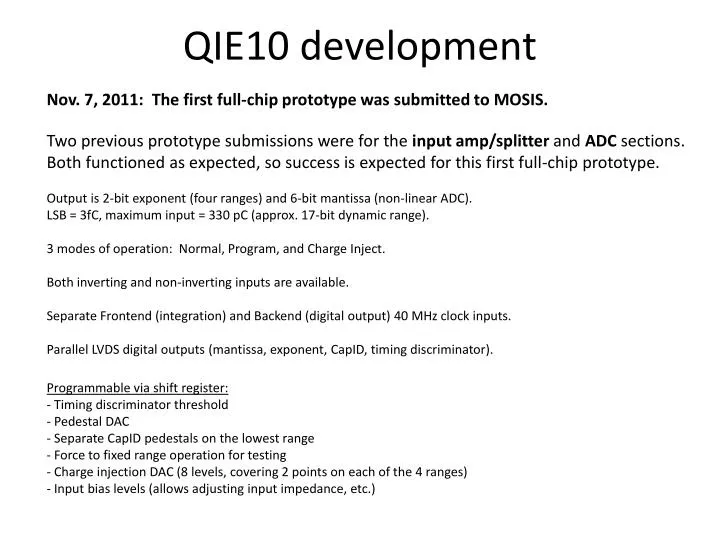
QIE10 development. Nov. 7, 2011: The first full-chip prototype was submitted to MOSIS. Two previous prototype submissions were for the input amp/splitter and ADC sections. Both functioned as expected, so success is expected for this first full-chip prototype.

E N D
QIE10 development Nov. 7, 2011: The first full-chip prototype was submitted to MOSIS. Two previous prototype submissions were for the input amp/splitter and ADC sections. Both functioned as expected, so success is expected for this first full-chip prototype. Output is 2-bit exponent (four ranges) and 6-bit mantissa (non-linear ADC). LSB = 3fC, maximum input = 330 pC (approx. 17-bit dynamic range). 3 modes of operation: Normal, Program, and Charge Inject. Both inverting and non-inverting inputs are available. Separate Frontend (integration) and Backend (digital output) 40 MHz clock inputs. Parallel LVDS digital outputs (mantissa, exponent, CapID, timing discriminator). Programmable via shift register: - Timing discriminator threshold - Pedestal DAC - Separate CapID pedestals on the lowest range - Force to fixed range operation for testing - Charge injection DAC (8 levels, covering 2 points on each of the 4 ranges) - Input bias levels (allows adjusting input impedance, etc.)
Digital Output Sync 6-bit mantissa Non-linear ADC (“6-bit”) Pad frame/ ESD protection 4-phase analog and digital MUX 2-bit Exponent 2-bit CapID Digital bypass Clock buffers 4-phase ring counter Mode select (Normal, Program, or Charge Inject) Range Select and MUX 4 ranges, scaled by X8 Range2 Range0 Range1 Range3 Serial program shift register Integrators Bias Power-up reset Bandgap reference Timing discriminator Input amps/splitters QIE10 schematic Programmable CapID pedestals (lowest range) Charge Injection Inverting Input Non-inverting Input Programmable Input Bias
LVDS outputs (6 bits mantissa, 2 bits exponent, 2 bits CapID) Mode control Serial program shift register Digital power Serial program in Serial program out ADC Digital Bypass Digital LVDS Inputs (FEck, BEck, Reset) Bandgap Ref. Ring Analog power (5V, 3.3V) Range select Timing discriminator LVDS out Integrators Input Bias Bias Charge Inject Non-inverting input bias Timing Disc. Inverting input bias Inverting amp/splitter (positive current) Non-inverting amp/splitter (negative current)