Download
1 / 21
210 likes | 292 Vues
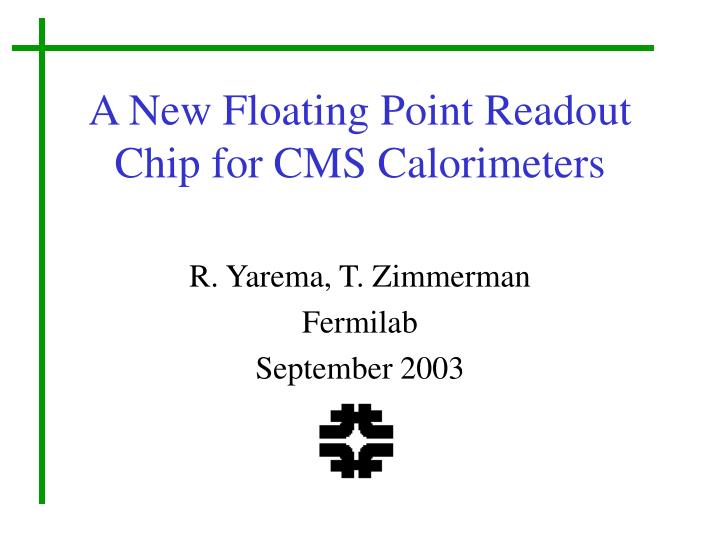
A New Floating Point Readout Chip for CMS Calorimeters. R. Yarema, T. Zimmerman Fermilab September 2003. Introduction. The Floating Point Readout Chip for CMS Hadron Calorimeters is the latest in a series of QIE chips designed at Fermilab for processing signals. It is called QIE8.

E N D
A New Floating Point Readout Chip for CMS Calorimeters R. Yarema, T. Zimmerman Fermilab September 2003
Introduction • The Floating Point Readout Chip for CMS Hadron Calorimeters is the latest in a series of QIE chips designed at Fermilab for processing signals. It is called QIE8. • QIE stands for Charge (Q) Integrator and Encoder. • A QIE is a custom integrated circuit that accepts a signal from a source such as a PMT or HPD and digitizes the signal. 9th Workshop on Electronics for LHC
CMS Hadron Calorimeter Front End Readout Module • Two QIE8 chips interface to each CCA (channel control ASIC) chip (See LHC 2002) • The CCA sends control signals to the QIE8 and accepts data from the QIE8. • 3 CCAs feed data to 2 GOLs 9th Workshop on Electronics for LHC
Hadron Calorimeter Front End Module QIE CCA GOL 9th Workshop on Electronics for LHC
QIE8 Chip Development • QIE8 designed in AMS 0.8 µm BiCMOS process. • First version of chip had a major problem in that operation at 40 MHz was marginal at best. • Problem traced to poor model of P-channel devices. • AMS later acknowledged problem and provided new models. • Second version of the chip was redesigned for different PMOS models and included significant layout changes needed to achieve desired performance. • The second version was the production order!! 9th Workshop on Electronics for LHC
QIE8 Basics • QIE8 can be programmed to accept either positive (PMT) or negative (HPD) input charge by powering the appropriate input. • QIE8 operates in a 4 step pipeline mode. • QIE8 digitizes input signal over a wide dynamic range and provides the necessary resolution for CMS. • The QIE8 has an embedded non-linear 5 bit FADC. • The data is output as a 2 bit exponent and 5 bit mantissa along with the time slice information, which is referred to as Cap ID. 9th Workshop on Electronics for LHC
Range Code • 5) The range code forms the exponent. • 4) For a given input charge, one appropriate range output is selected and digitized by an ADC, forming the mantissa. • 3) Splitter ratios and integration C ratios are chosen to achieve range-to-range scaling of the transfer gain (I/C) by factor A. • 2) Each splitter range output feeds a charge integrator. The current fractions are integrated simultaneously on all ranges. • 1) Input current pulses are divided into weighted fractions by a current splitter The QIE in a Nutshell 9th Workshop on Electronics for LHC
HPD (positive) input QLSB = 1 fC (normal mode) QLSB = 0.33 fC (cal. Mode) Input impedance < 40 Ω Input analog BW > 20 MHz ENC (Cin = 30 pF) <0.5 fC PMT (negative) input QLSB = 2.7 fC (norm mode) QLSB = 0.9 fC (cal. mode) Input impedance = 50/93 Ω Input BW > 40 MHz ENC (5m, 50 Ω cable), 2fC QIE8 Specifications Resolution = 2% QMAX/QLSB = 10,000 (>13 bits) Beam crossing time = 25 nsec ADC DNL (small signals) <0.05 LSB 9th Workshop on Electronics for LHC
Design Challenges • Custom FADC with very low DNL • Mixed mode analog/digital design • Must respond to positive and negative inputs. • Single power supply for easy operation • Controlled impedance inputs • High sensitivity inputs (1 fC/LSB for HPD) • Very high sensitivity calibration mode (1/3 fC/LSB to track detector response shifts from radioactive source (200 e). 9th Workshop on Electronics for LHC
QIE scheme: Range integrators are offset If range integrators not offset: all ranges intersect at the origin “Modified” floating point format A = 2: standard floating point (All ranges except the lowest use half the ADC span) More efficient: each range uses the full ADC span) QIE8 Uses A Modified Floating Point Design 9th Workshop on Electronics for LHC
Resolution (Relative Quantization Error) Example: A = 2 N = 8 bits QLSB = 1fC 8 ranges Standard floating Point design Modified floating Point design Modified floating point with A = 2: 2x smaller error, 2x more range! 9th Workshop on Electronics for LHC
Design Strategy • In order to have a sensitive and fast input, the number of transistors in the input splitter needs to be minimized. • To reduce the number of transistors, use fewer ranges (which requires a larger range scaling factor, A) • Choose 4 ranges (5:1:1:1 splitter ratio) and range scaling A = 5 • Perform range scaling mostly with integration capacitor ratios instead of current splitter ratios. • Number of ADC bits • Uniform ADC requires 6 bits to meet resolution requirement • A non-uniform ADC can achieve same resolution with only 5 bits • Use 5 bit non-uniform ADC • To reduce bits in data output. • To simplify ADC design (fewer comparators) 9th Workshop on Electronics for LHC
Block Diagram Pseudo-differential QIE configuration: Signal applied between SIG input and ground, REF input is “dummy.” QIE insensitive to bias, temp, supply V, common mode noise PMT input HPD input 9th Workshop on Electronics for LHC
Different Input Amps for PMT and HPD Negative input (PMT) Signal Reference Positive input (HPD) Gain = -2.7 Signal Reference Note: a 4 range (5:1:1:1) splitter uses only 8 transistors 9th Workshop on Electronics for LHC
Integrators and Range Select Circuits Thermometer code output To FADC From Current Splitters 9th Workshop on Electronics for LHC
Custom Pseudo Differential, Non-uniform ADC Preamps with output averaging for low DNL 9th Workshop on Electronics for LHC
Digital outputs (low level differential) Digital bypass caps (650 pF total) Digital power, control inputs Analog power, bias Analog/digital substrate isolation technique: N collector implant (connect to +5V) Substrate contact (dedicated gnd pin) Analog inputs (pseudo-diff.) Die size: 3.0 x 4.3 mm 9th Workshop on Electronics for LHC
Production Testing • Received 25,079 packaged parts • Built robot chip tester (4 months) to handle parts • Eliminates Post Doc burn out • Insures bad parts are sorted properly • Minimizes damage to pins due to handling • Tester holds 7 trays with 160 QIE8s per tray • Tests all QIE8 functions • 18 major tests • Each test test may include hundreds of measurements 9th Workshop on Electronics for LHC
QIE8 Chip Tester 9th Workshop on Electronics for LHC
Test results Radioactive source calibration test: each point is 500,000 acquisitions (14 ms) averaged. • Meets all specifications • Runs at > 70 MHz • Low DNL (< 0.05 LSB in normal mode) • Power = 330 mw from single 5.0 V supply. • Stable against shifts in bias, temp, clock, Vdd, etc. • No digital coupling to inputs if board is laid out properly (tricky). • Need 8200 +1800 parts for HPDs and PMTs. Expect 19,500 good parts. (Yield=78%) 180 e 7 sec 9th Workshop on Electronics for LHC
Summary • Production quantity of QIE8 chips has been received. • All chips have been packaged. • Testing with newly developed robot is proceeding. • The robot has been so successful that a second robot is being built. • QIE8 parts meet specifications. • Yield is good. 9th Workshop on Electronics for LHC