Download
1 / 32
320 likes | 528 Vues
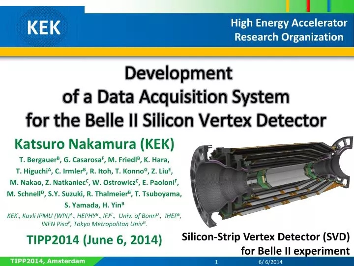
Development of a Data Acquisition System for the Belle II Silicon Vertex Detector. Katsuro Nakamura (KEK) T. Bergauer B , G. Casarosa F , M. Friedl B , K. Hara, T. Higuchi A , C. Irmler B , R. Itoh , T. Konno G , Z. Liu E ,

E N D
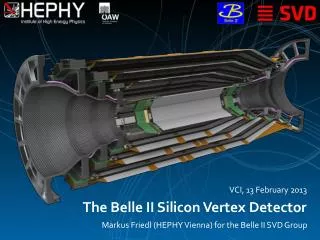
Developmentof a Data Acquisition Systemfor the Belle II Silicon Vertex Detector Katsuro Nakamura (KEK) T. BergauerB, G. CasarosaF, M. FriedlB, K. Hara, T. HiguchiA, C. IrmlerB, R. Itoh, T. KonnoG, Z. LiuE, M. Nakao, Z. NatkaniecC, W. OstrowiczC, E. PaoloniF, M. SchnellD, S.Y. Suzuki, R. ThalmeierB, T. Tsuboyama, S. Yamada, H. YinB KEK、Kavli IPMU (WPI)A、HEPHYB、IFJC、Univ. of BonnD、 IHEPE, INFN PisaF, Tokyo Metropolitan UnivG. TIPP2014 (June 6, 2014) Silicon-Strip Vertex Detector (SVD) for Belle II experiment TIPP2014, Amsterdam
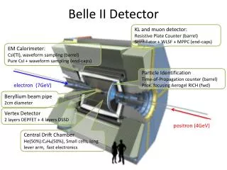
Belle II Experiment andSilicon-Strip Vertex Detector Belle II detector Silicon-Strip Vertex Detector(SVD) • Belle II experiment (SuperKEKB) • GeV collider • designed luminosity: cm-2s-1 • max. trigger rate: 30 kHz • search for the physics beyond the SM • Detectors and accelerator are being developed toward start at 2016 • 4-layer DSSD sensors • measure 2D track position for charged particles • more than 220,000 readout strips • SVD provides RoI (region of interest) in the inner 2-layer Silicon-Pixel Vertex Detector (PXD) • PXD data reduction and accurate track reconstruction charged particle GeV GeV GeV GeV SuperKEKB @ KEK DSSD TIPP2014, Amsterdam
APV25 and Requirement on Triggers APV25 chip output from APV25 (6 samples/trigger) ADC ✔ discussed later ✔ ✔ 1 sample a particle hit ✔ clock tick (32MHz) • APV25 chip • Front-end electronics for DSSD signal readout • Provides 128-channels analog signals sampled among several clock ticks • Shaping time: 50 nsec • Suitable for high occupancy in Belle II SVD • 6- and 3-samples/trigger modes will be used for Belle II SVD • 6-samples/trigger is preferable for good peak finding • Requirements on triggers from APV25 • Maximum trigger rate: (140 clocks/sample) • 38kHz (6-samples), 76kHz (3-samples) • cf. max. trigger rate in Belle IIis30kHz • Minimum trigger interval: (3 clocks/3-samples) • 189nsec (6-samples), 94nsec (3-samples) • Maximum trigger latency: • 5.0 usec (available pipe-line size of 160 samples) TIPP2014, Amsterdam
SVD Readout System Overview FADC x48 Junction boxes ( signal repeater ) ~2m copper cables ~10m copper cables Belle II DAQ Belle II SVD data flow HSLB data format zero-sup. flash ADC basf2 FTBx48 DAQ belle2link B2L data format Aurora control signals Aurora link 1748 APV25’s VME backplane Buffer x4 calculate RoI on-line clock, trigger, reset … PXD RoI belle2tt clock, trigger, reset … PXD system copper cables FADC-Ctrl belle2tt B2TT decoder FADC control APV Trig. Gen. APV25 chips Belle II trigger/ timing controller clock, trigger, reset … SVD readout system SVD readout system is driven by 32MHz clock. TIPP2014, Amsterdam Performance of the readout system has to be confirmed with prototypes before final production.
Development of Prototype FADC Board prototype FADC board VME 9U signals from 48 x APV25 FTB board • High signal density • readout 48 APV25 outputs • APV25signal processing on FADC • analog level conversion (AC coupling) • 10-bit ADC • FPGA (Stratix IV)data processing • FIR filter • Common-Mode Correction • Zero-Suppression • data transmission to FTB TIPP2014, Amsterdam
Development of Prototype FADC Board hit information from APV25chip (6-samples/trigger) ADC average of ADC shifts from pedestal Common-ModeCorrection Clock Ticks (32MHz) CMC distribution (n-side) ADC distribution before CMC ADC distribution after CMC obtained from raw ADC data obtained from raw ADC data after CMC typical MIP: 70 ADC typical MIP: 70 ADC [ADC] TIPP2014, Amsterdam • Zero-Suppressionfunction • Only transmits hits above threshold • Threshold is recoded in the FPGA memory • Two steps of CMC (Common-ModeCorrection) before zero-suppression • calculates average of ADC shifts from pedestals • Successfully prepared hardware and firmware for the FADC prototype.
Development of Prototype FTB prototype FTB board VME 3U JTAG port SFP port DAQ SFP port data from FADC SFP port PXD FPGA Xilinx SPARTAN-6 SC signal receiver Stability test for serial lines with PRBS-7 FTB FTB connect SFP ports each other • Finesse Transmitter Board (FTB) • FTB main feature: high speed serial communication with other systems • line to DAQ: 2.5 Gbps • line to PXD:1.3 Gbps • Stability test for the serial lines • with 3.175 Gbps PRBS-7 • No errors were observed during an 8-day long bench test with a 2-FTB system. • This result corresponds to 11 days of correct SVD data transmission with a 48-FTB system in 95% C.L. • assuming 1kB event size from an FADC board and 30 kHz trigger rate. TIPP2014, Amsterdam
Other Componentsin SVD Readout System FADC x48 Junction boxes ( signal repeater ) ~2m copper cables ~10m copper cables Belle II DAQ Belle II SVD data flow HSLB data format zero-sup. flash ADC basf2 FTBx48 DAQ belle2link B2L data format Aurora control signals Aurora link 1748 APV25’s VME backplane Buffer x4 reduction of PXD data size clock, trigger, reset … FTSW PXD RoI belle2tt clock, trigger, reset … PXD system copper cables FADC-Ctrl belle2tt B2TT decoder FADC control APV Trig. Gen. APV25 chips trigger/ timing distributer clock, trigger, reset … SVD readout system TIPP2014, Amsterdam Prototypes of all other remaining components have been developed as well. An integrated SVD readout test was performed with the full system.
SVD Readout Test at DESY Beam Line 4-layertest SVDmodules DESYbeam line APV25chips in light-shielding box beam (2 - 6 GeV) DSSDsensor test SVDmodules Superconducting solenoid magnet (max. 1T) TIPP2014, Amsterdam
SVD Readout System at Beam Test SVD readout system Belle II DAQsetup FADCboard • same readout chain as Belle IIexperiment • first test of the full readout chain • trigger rate: ~ 400 Hz • confirmation of correct data processing • event number check • CRC checksum • Stable operation of the readout during the beam test (about 3 weeks) JTAGserver PXD-DatConsystem FTBboard TIPP2014, Amsterdam
Analysis Results from Beam Test Data event display observed performance of SVD module • From the resulting high efficiency, we confirmed our CMC and zero-suppression do not lose SVD hit efficiency. cluster charge distribution cluster size distribution peak: corresponds to about 22,000 SVDmodules reconstructed track w/ magnetic field cluster hit efficiency for tracks cluster hit efficiency for tracks efficiency efficiency: 99.4% position of track projection[cm] TIPP2014, Amsterdam
APV25 Trigger-FIFO and APV25-FIFO Emulator Implement ‘ APV25-FIFO emulator ’ trigger signals to all sub-systems Belle II SVD global trigger decision veto APV25 trigger-FIFO APV25-FIFO emulator threshold for trigger veto Belle II trigger/timing controllermodule: global decision of Level-1 trigger accept APV25 chips 32 samples emulated FIFO occupancy emulated FIFO occupancy 32 samples TIPP2014, Amsterdam • Data transmission in 6-samples mode takes 26.5 usec/trigger and one in 3-samples mode takes 13.2 usec/trigger. • The transmission dead time is absorbed by trigger-FIFO in APV25. Available trigger-FIFO depth in APV25 is 32 samples. • FIFO overflow has to be avoided. • ‘APV25-FIFO emulator’ calculates the trigger-FIFO occupancy, and asserts a trigger veto in order to stop trigger and avoid FIFO overflow. • The APV25-FIFO emulator is to be implemented in future. • Trigger dead time from this veto system has to be considered.
Simulated Trigger Dead Timefrom APV25-FIFO Emulator Trigger dead time vs. Raw trigger rate (Simulation) Belle II designed max. trigger rate only 6-samples : fraction of mixed 3-samples mode only 3-samples threshold: 26 samples no trigger/busy propagation trigger interval: 190nsec (24 clocks) Trigger dead time at 30 kHz trigger is 3%.This is acceptable. Furthermore, the trigger dead time can be decreased by switching btw. 3-/6-samples event-by-event according to trigger timing resolution. If we can increase to more than 0.7, 50 kHz trigger is also acceptable. TIPP2014, Amsterdam
Schedulefor Readout System Development Schedule FADC board • Jul. 2014: prototypever.2 • fix minor bugs on PCB • implementation of APV25-FIFO emulator • Nov. 2014:prototypever.3(if necessary) • start production from the beginning of 2015 FTB board • Hardware/firmware are already developed well. • production from the end of 2014 Full readout system will be built up in 2015 toward the start of Belle II experiment in 2016. TIPP2014, Amsterdam
Summary and Outlook • The SVD readout system are being developed toward the start of Belle II at 2016. • Prototypes for FADC, FTB, and all other components were prepared. • Common-ModeCorrection+ Zero-Suppression • stability test for high speed serial link with 3.175Gbps PRBS-7 • Successful SVD readout test at DESY beam line was performed. • full readout chain test at the first time • Stable operation was confirmed by checking event numbers and CRC check-sums. • Excellent performance of the SVD module was observed. • Expected trigger dead time at 30 kHz trigger rate is 3% (acceptable). • By increasing 3-samples trigger fraction, we can decrease the dead time. We confirmed that the SVD readout system provides excellent performance for the Belle II experiment. • We will apply minor modifications on FADC board and start the mass production at the beginning of 2015. TIPP2014, Amsterdam
Thank you! TIPP2014, Amsterdam
DAQ limitations from APV25 • Trigger rate • 1 sample data transmission to FADC takes 140 clock cycles. • 3-sample mode Maximum trigger rate is 76kHz • 6-sample mode Maximum trigger rate is 38kHz • cf. The target trigger rate in Belle IIis30kHz. • 6-sample mode works fine in low luminosity, but combination of 3- and 6-samples have to be used in higher luminosity. • Minimum trigger interval • 1 trigger reception needs 3 clock cycles for 3-sample mode and 6 clock cycles for 6-sample mode. • 3-sample mode Minimum trigger interval is ~94 nsec. • 6-sample mode Minimum trigger interval is ~190 nsec. • CDC also requires 200 nsec separation. • Maximum triggerlatency • Maximum available pipeline depth is 160 clock cycles. • That requires trigger latency of less than 5 usec. • APV25 has FIFO with 32-samples depth • To avoid FIFO overflow, a finite trigger-dead-time has to be introduced. TIPP2014, Amsterdam
Junction box • Supply HV and LV to DSSDand APV25. • DC/DC converter • Joint signals between APV25 and FADC board. DC/DC converters 2 prototypes for p- and n-sides TIPP2014, Amsterdam
FADC data output format • Modes of operation: • Raw mode • raw ADC data for a defined length • Transparent mode • APV25 frame detection with header data and raw data of all strips • Zero-suppressed mode • Pedestal subtraction, CMC, only hits above threshold (3 or 6 samples) • Zero-suppressed/hit time finding mode (not implemented yet) • Peak sample and peak time, all 3 or 6 samples only for unclear cases (such as double peak = pileup) • Raw + transparent are typically used SVD-internally (timing adjustments, pedestal/noise evaluation, calibration, …) • Zero-suppressed (+hit time finding) are the normal data formats for physics data acquisition TIPP2014, Amsterdam
FADC datastream diagram ADC data of APV output APV frame detection data reordering ADC data decoder RAW data pipeline 512 cells raw mode data encoder CMC 1 transparent data encoder FIFO selector CMC 2 Data Transmitter for FTB x 48 APVs zero suppressed data Hit finder & encoder All the three data-modes are working well. TIPP2014, Amsterdam
FADC status monitoring APV header detection error ADC frame detection error APV FIFO full 32sample depth FIFO full 2k word depth Error status of FADC is important to guarantee the data correctness. The most probable error sources in firmware: TIPP2014, Amsterdam
Data format for zero-suppression new format for the beam test (from Jan. 21, 2014) old format Error-bits for the quality confirmation and diagnoses. TIPP2014, Amsterdam
FTB data format Current format Next format • The current data format works well. • A few improvements will be applied in future. • Confusing magic numbers in header and trailer will be changed. • Currently, they are same as the magic numbers in B2L header and trailer. • Trailing ‘0’ in the MSB 8-bits to distinguish all types of frames. • Leave all the FADC data as they are. TIPP2014, Amsterdam
FADC-Controller and Buffer boards Buffer board 1st prototype of FADC-Controller board buffers FPGA CYCLON II FADC-Controller board 4 Buffer board All FADC boards in a crate buffers FPGA STRATIX IV GbE interface FTSW • We will have 4 crates with FADC modules • One has single FADC-Controller • Receives FTSW signals • Distributes clock, trigger and other controls to all Buffer • Each crate has single Buffer module • Receives FADC-Controller signals • Distributes signals to FADCs through backplane bus TIPP2014, Amsterdam
Pedestal and gain calibration TuxDAQ calibration signal particle signal APV25 output TuxOA hit map • TuxDAQ + TuxOA • C++ application • Linux 32/64 bit • Used at DESY beam test • TuxDAQ • SVD standalone DAQ • Samples data on FADC data-stream • noise data • gain calibration data • as well as physics data • Configures parameters in FADC system • ADC clock delay scan • TuxOA • Simple analyses of sampled FADC data • Noise and pedestal • gain calibration constants • Hit profile (chip / module level) • Worked well at DESY TIPP2014, Amsterdam
SVD Run/Slow Control SVD run control GUI SVD HV/LV control GUI Integration plan of SVD run/slow control • PXD and IBBelle will employ EPICS, and SVD shares CO2 cooling system and environmental monitors with PXD • SVD will be involved in the EPICS control system. • Common data logging on EPICS database • EPICS integration on our software needs to be done. TIPP2014, Amsterdam
SVD rack location at IR SVD FWD SVD BWD TIPP2014, Amsterdam
Manpower for development M. Friedl (HEPHY):System & schematics design, supervision S. Schmid (HEPHY):CAD schematics & PCB layout J. Pirker (HEPHY):Parts purchasing, assembly (soldering) M. Eichberger (HEPHY): Assembly (soldering, wire bonding) C. Irmler (HEPHY): Assembly (wire bonding), software supervision, Origami/hybrid testing R. Thalmeier (HEPHY): FADC hardware and firmware H. Yin (HEPHY): Online software W. Ostrowicz (Cracow): FTB hardware and firmware Z. Natkaniec (Cracow): FTB hardware and firmware M. Schnell (Bonn): FTB DatCon interface firmware K. Nakamura (KEK): Firmware, B2Link/B2TT, System integration at KEK TIPP2014, Amsterdam
Comparison with simulation live ratio: 20% dead time • Trigger dead time from the FTSW “pipeline busy” is simulated. • Simulation with LFSR (linear feedback shift register) pattern generator, which is really used in FTSW, well describes the measured live ratios. • There is no other big dead time sources in our system. • Green curve shows expected live ratio with Poisson distribution triggers (real triggers) • Dead time is expected to be about 20% at 30kHz. Too large for the Belle II operation. • APV25 emulator would be necessary for our busy handling. TIPP2014, Amsterdam
Residual distribution(CMC16, tight cut) fitting function: p-side n-side determined cut region as determined cut region as NO. NAME VALUE ERROR SIZE DERIVATIVE 1 p0 3.63112e+03 1.91311e+01 4.04379e-05 2.35151e-02 2 p1 1.63427e-03 6.42714e-05 8.53023e-07 -1.94406e+00 3 p2 1.45968e-02 7.25321e-05 2.10705e-05 1.11957e-01 4 p3 1.64809e+02 1.00714e+01 7.75674e-05 1.72498e-02 5 p4 3.53879e-04 5.49890e-04 7.27532e-06 -2.24539e-01 6 p5 4.14886e-02 9.68568e-04 5.59383e-05 1.09194e-02 NO. NAME VALUE ERROR SIZE DERIVATIVE 1 p0 3.23921e+03 1.94809e+01 2.08186e-05 -5.55985e-03 2 p1 1.32647e-04 3.78820e-05 2.73072e-07 -3.97456e-01 3 p2 7.97590e-03 4.79511e-05 1.34153e-05 7.85978e-03 4 p3 2.60344e+02 1.42551e+01 4.32121e-05 7.62981e-03 5 p4 2.23610e-04 2.20931e-04 1.59234e-06 -4.49666e-01 6 p5 2.04253e-02 3.89271e-04 2.40944e-05 1.84963e-02
Intrinsic efficiency for cluster finding in L3(CMC16, tight cut) red: # of extrapolations blue: # of associated clusters after previous cut (|x|<8*p2) p-side n-side division division p-side n-side (*) The red lines are not fitting results,but just result of division of entries. Efficiency is more than 99% in both p-side and n-side.
CMC dependence p-side CMC128 CMC32 CMC16 CMC128 CMC32 CMC16 n-side