Download
1 / 9
90 likes | 220 Vues
Microplasma Optical Emission Spectrometer (MOES) on a chip. SFR Workshop November 8, 2000 Michiel Krüger, David Hsu, Scott Eitapence, K. Poolla, C. Spanos, D. Graves, O. Solgaard Berkeley, CA.

E N D
Microplasma Optical Emission Spectrometer (MOES) on a chip SFR Workshop November 8, 2000 Michiel Krüger, David Hsu, Scott Eitapence, K. Poolla, C. Spanos, D. Graves, O. Solgaard Berkeley, CA 2001 GOAL: to build a microplasma generating system and test it with bulk optical components by 9/30/2001.
Motivation and background • Motivation • Precise detection of compounds near substrate required during semiconductor manufacturing • Organic compounds, emitted during DUV, can coat optics of stepper • Background • Small atmospheric pressure glow discharges can be used for species excitation. • Glow discharge optical emission spectroscopy has long history in analytical chemistry
Microplasma Optical Emission Spectrometer • Basic idea: • OES from plasma reveals info about gas composition in chamber • Interdisciplinary: • plasma physics and chemistry • MEMS processing • optics and metrology • Inter-departmental: • chemical engineering • electrical engineering • mechanical engineering
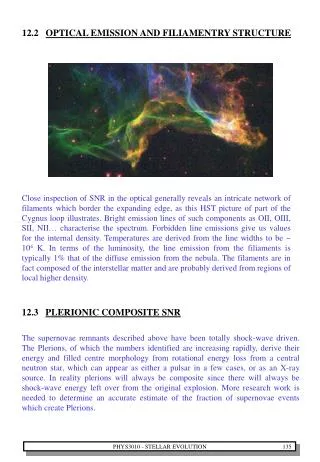
plasma cathode mm dielectric anode MOES (cont.) • Generation of plasma with hollow cathode • Generation of plasma possible if: 0.05<p.D<10Torr.cm • Smaller diameter (75 mm) allows plasma generation at atmospheric pressure! • This results in smaller sensor • Many applications in (and outside!) IC processing industry (for example in lithography) D
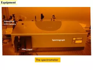
grating detector array lens Schematic of initial MOES experimental configuration • Combination of • Bulk optical optical components • Microplasma chamber, fabricated in Si substrate • Light emitted from discharge is captured by lens and collimated onto grating • Diffracted light from grating is focused on detector array to record spectrum
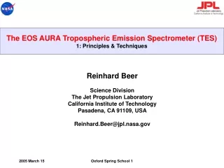
Molybdenum anode Mica dielectric (drilled hole) Silicon chip with 200mm hole and aluminum cathode First experiments: plasma in 200mm hole, 100Torr N2 ambient molybdenum chip mica dielectric vacuum chamber
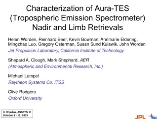
50-200m 0.7m poly-Si 1m SiO2 200m substrate Currently fabricated in UCB Microlab • Relatively simple to make • XeF2 etch to achieve required depth and undercut • Very small diameters, i.e. high pressure, possible plasma cathode anode
Fabrication process and challenges • Fabrication • OES cavity defined by deep reactive ion etching/XeF2 isotropic etch • anode/cathode defined on front and backside of wafer (metal or doped Silicon) • Challenges • Microplasma stability and contamination • Device sensitivity • Packaging of device • Exploration of pulsed operation to make autonomous power supply possible • Integration of micro discharges onto chips for other applications
2002 and 2003 Goals Build micro-optics for spectral analysis. Complete the preliminary designs for integrated MOES, by 9/30/2002. Design and test integrated MOES. Calibration studies, sensor characterization, by 9/30/2003.