Download

1 / 14
180 likes | 482 Vues
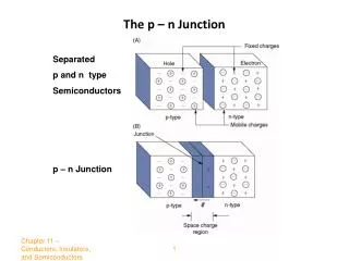
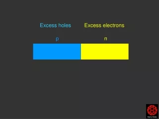
P-N JUNCTION. Single piece of SC material with half n- tpye and half p-type The plane dividing the two zones is called junction (plane lies where density of donors and acceptors is equal). P-N JUNCTION. P. N. -. -. -. +. +. +. -. -. -. +. +. +. -. -. -. +. +. +. Junction.

E N D
Single piece of SC material with half n-tpye and half p-type • The plane dividing the two zones is called junction (plane lies where density of donors and acceptors is equal) P-N JUNCTION P N - - - + + + - - - + + + - - - + + + Junction • Three phenomenas take place at the junction • Depletion layer • Barrier potential • Diffusion capacitance
Formation of depletion layer • Also called Transition region • Both sides of the junction • Depleted of free charge carriers • Density gradient across junction (due to greater difference in number of electrons and holes)-Results into carrier diffusion • Diffusion of holes (from p to n) and electrons (from n to p) • Diffusion current is established • Devoid of free and mobile charge carriers (depletion region) • It seems that all holes and electrons would diffuse!!! P-N JUNCTION
But this does not happen • There is formation of ions on both sides of the junction • Formation of fixed +ve and –ve ions- parallel rows of ions • Any free charge carrier is either • Diffused by fixed ions on own side • Repelled by fixed ions of opposite side • Ultimately depletion layer widens and equilibrium condition reached - - + + - - + + P N - - + + - + - + - +
Inspite of the fact that depletion region is cleared of charge carriers, there is establishment of electric potential difference or Barrier potential (VB) due to immobile ions BARRIER VOLTAGE P N - + - - + + - + - - + + - + - - + + VB
VB for Ge is 0.3eV and 0.7eV for Si • Barrier voltage depends on temperature • VB for both Ge and Si decreases by about 2 mV/0C Therefore VB= -0.002 t where t is the rise in temperature • VB causes the drift of carriers through depletion layer. Hence barrier potential causes the drift current which is equal and opposite to diffusion current when final equilibrium is reached- Net current through the crystal is zero PROBLEM • Calculate the barrier potential for Si junction at 1000C and 00C if its value at 250C is 0.7 V
Explanation of P-N junction on the basis of Energy band theory • Operation of P-N junction in terms of energy bands • Energy bands of trivalent impurity atoms in the P-region is at higher level than penta-valent impurity atoms in N-region (why???) • However, some overlap between respective bands • Process of diffusion and formation of depletion region • High energy electrons near the top of N-region conduction band diffuse into the lower part of the P-region conduction band • Then recombine with the holes in the valence band • Depletion layer begins to form • Energy bands in N-region shifts downward due to loss of high energy electrons • Equilibrium condition- When top of conduction band reaches at same level as bottom of conduction band in P-region- formation of steep energy hill
CB CB CB CB VB VB VB VB P-Region N-Region P-Region N-Region
Forward Biasing • Positive terminal of Battery is connected with P-region and negative terminal with N-region • Can be explained by two ways. One way is • Holes in P-region are repelled by +ve terminal of the battery and electrons in N-region by –ve terminal • Recombination of electrons and holes at the junction • Injection of new free electrons from negative terminal • Movement of holes continue due to breaking of more covalent bonds- keep continuous supply of holes • But electron are attracted to +ve terminal of battery • Only electrons will flow in external circuit Biasing of P-N junction
P N - + - - + + - + - - + + - + - - + +
Another way to explain conduction • Forward bias of V volts lowers the barrier potential (V-VB) • Thickness of depletion layer is reduced • Energy hill in energy band diagram is reduced • V-I Graph for Ge and Si • Threshold or knee voltage (practically same as barrier voltage) • Static (straight forward calculation) and dynamic resistance (reciprocal of the slope of the forward characteristics)
Reverse Biasing • Battery connections opposite • Electrons and holes move towards negative and positive terminals of the battery, respectively • So there is no electron-hole combination • Another way to explain this process is • The applied voltage increases the barrier potential (V+VB)- blocks the flow of majority carriers • Therefore width of depletion layer is increased • Practically no current flows • Small amount of current flows due to minority carriers (generated thermally) • Also called as leakage current • V-I curve and saturation
P N - + - - + + - + - - + + - + - - + +
Compute the intrinsic conductivity of a specimen of pure silicon at room temperature given that , and . Also calculate the individual contributions from electrons and holes. PROBLEMS • Find conductivity and resistance of a bar of pure silicon of length 1 cm and cross sectional area at 3000k. Given • A specimen of silicon is doped with acceptor impurity to a density of 1022 per cubic cm. Given that All impurity atoms may be assumed to be ionized • Calculate the conductivity of a specimen of pure Si at room temperature of 3000k for which The Si specimen is now doped 2 parts per 108 of a donor impurity. If there are 5x1028 Si atoms/m3, calculate its conductivity.