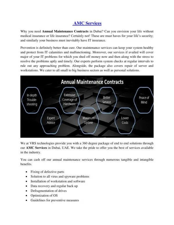
Download
1 / 7
70 likes | 151 Vues
8xADC AMC board. Tomasz Klonowski T.Klonowski@elka.pw.edu.pl Warsaw University of Technology PERG – ISE 3.12.2007. Requirements. 8xADC (100 MHz) + FPGA for d ata acquisition and processing Form factor: AMC.1 (with PCIExpress), single width

E N D
8xADC AMC board Tomasz Klonowski T.Klonowski@elka.pw.edu.pl Warsaw University of Technology PERG – ISE 3.12.2007
Requirements • 8xADC (100 MHz) + FPGA for data acquisition and processing • Form factor: AMC.1 (with PCIExpress), single width • ADC: 14-16 bit, ~100 MHz sample rate, conversion time 7 maximum clocks • FPGA: Virtex 5 with external memory (2-4 MB, 250 MHz) • 2 EEPROMs for FPGA • 2 different clocks (configurable) for ADC 1-4 and ADC 5-8 • clock distribution stability better than 5 ps • IPMI • additional signals from rear • 8x analog signal 50-100 MHz through signal conditioning connected to ADC • 6x clock up to 100 MHz, LVDS bus, jitter less than 5 ps • 2 of them connected to FPGA and ADC (user can choose clock for ADCs) • 4 clocks connected to FPGA, LVDS bus
AMC connector A+ AMC connector B+ Analog signals 1-8 Data 8 bits PCI Express JTAG I2C Clocks 1-2 uC Atmega 128 inhibit Power supply Interconnector Clocks 3-6 Signal conditioning band-pass filters JTAG Data 8 bits Clock distribution AD9510 AD9513 EEPROM XCF16P ADC 1-4 AD6645 ADC 5-8 AD6645 Hot -swap switch FPGA Virtex5 XC5VLX30T Data 8x16 bits Clocks 1-2 Clocks 3-6 Clock configuration bus Data enable Buffers Interconnector Data 36 bits Data 8x16 bits QDR II SRAM 512K x 36 IDT71P74604 Board with analog and clock distribution components Board with digital and IPMI components Block Diagram
Functional • ADC AD6645 - 14-bit, 80 – 105 MSPS, conversion time 4 maximum clocks, • FPGA - Virtex 5 XC5VLX30T • QDR II SRAM IDT71P74604 18 Mb, 250 MHz • EEPROM XCF16P for FPGA – two configurations • IPMI • Clock distribution AD9510, AD9513 – configured by FPGA • clock distribution stability better than 5 ps • 2 different clocks for ADC 1-4 and ADC 5-8 • clocks configured by FPGA • Buffers – 74LCX574 – for latching data from converters
Interface • 8x analog signal 50-100 MHz through signal conditioning connected to ADC • 6x clock up to 100 MHz, LVDS bus • 2 of them connected to FPGA and ADC (user can choose clock for ADCs) • 4 clocks connected to FPGA, LVDS bus • IPMBus • Data 8 bits bus
Stage of work • All schematics are done • Layouts are expected to be finished by the end of January • The prototype board is expected to be started by the end of February • Tests of the protoype board are expected to be done by the and of April