Download
1 / 12
130 likes | 446 Vues
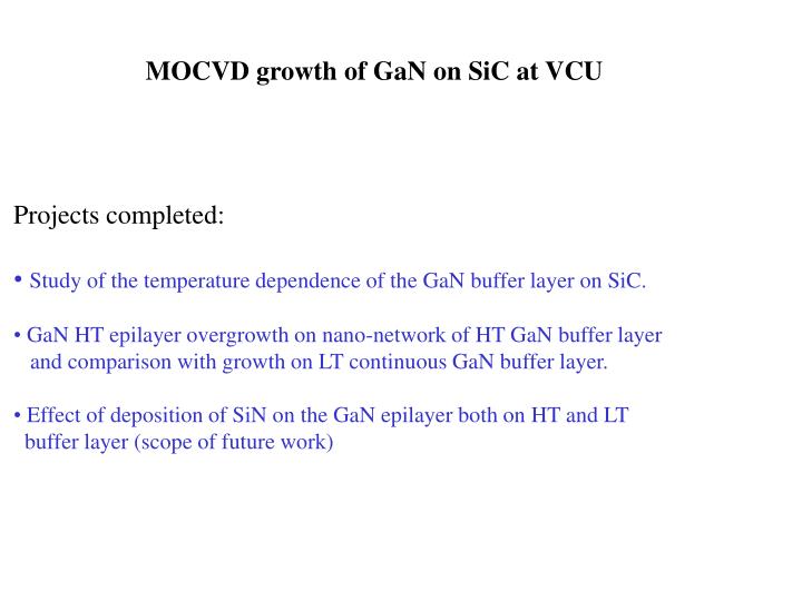
MOCVD growth of GaN on SiC at VCU. Projects completed: Study of the temperature dependence of the GaN buffer layer on SiC. GaN HT epilayer overgrowth on nano-network of HT GaN buffer layer and comparison with growth on LT continuous GaN buffer layer.

E N D
MOCVD growth of GaN on SiC at VCU • Projects completed: • Study of the temperature dependence of the GaN buffer layer on SiC. • GaN HT epilayer overgrowth on nano-network of HT GaN buffer layer • and comparison with growth on LT continuous GaN buffer layer. • Effect of deposition of SiN on the GaN epilayer both on HT and LT • buffer layer (scope of future work)
Temperature dependence of the GaN buffer layer on SiC • GaN buffer layer deposited on 6H-SiC, 3.50 miscut samples at four different temperatures: • 5650 C (~temp. used for buffer layer deposition on sapphire, reference (a) • 9000 C • 9500 C • 9700 C (~temp. range recently reported in reference (a) below) • Thin solid films, 289 (1996), 256 • J. Cryst. Growth, 248 (2003), 533
Temperature dependence of the GaN buffer layer on SiC 900 0 C, 7 min 950 0 C, 4.5 min • Buffer layer at 5650 C showed featureless • continuous surface in SEM. 970 0 C, 4.5 min
Temperature dependence of the GaN buffer layer on SiC • XRD data of the buffer layer on SiC. • Conclusion: HT buffer layer at 9500 C is the optimum for epilayer growth.
HT epilayer growth on LT (5650 C) and HT (9500C) buffer layer 400 nm of HT (10500) epilayer GaN was deposited on 100 nm of both LT (5650 C) and HT(5650 C) buffer Layer to study the effect of the buffer layer on the quality on the overgrown film. • XRD data: • Conclusion: Based upon the xrd data, there is a significant improvement on the epi-layer • quality grown on HT buffer layer. This may be due to two reasons: • The starting buffer layer quality is better for HT buffer layer. • Lateral overgrowth taking place in the film grown on the nano-network of the HT buffer • layer, as opposed to the growth on a continous LT GaN buffer layer, as shown in the SEM • images on the next two slides.
HT epilayer growth on LT (5650 C) and HT (9500C) buffer layer (continued from the previous slide) • SEM: • - HT epilayer on the continuous LT buffer layer showed a continuous featureless • epilayer. • - HT epilayer on the “nano-network” buffer layer at 9500 C showed a continuous • epilayer but with pinholes. These pinholes result from the partial coalescence of the • GaN epilayer after nucleating at nano network the buffer layer. 400 nm epi layer at 10500 C on 9500C buffer layer. 100 nm buffer layer at 9500C
HT epilayer growth on LT (5650 C) and HT (9500C) buffer layer (continued from the previous slide) To study the evolution these pinholes, two HT epilayers of different thickness (200 nm and 400 nm) were grown on the HT nano-network buffer layer. The following SEM image shows that the density of these pinholes decreased significantly with the thickness of the epilayer. In addition, these pinholes are hexagonal in shape (more visible in the 400 nm thick layer) whose walls are in the a-direction, the direction of the lateral overgrowth. 100 nm buffer layer at 9500C 200 nm epi-layer at 10500C 400 nm epi-layer at 10500C
10500 C 9500 C IV VII I II III V VI VIII time • 13.5 min. temp ramp-up. • 3 min. temp stabilization • 4.5 min. buffer layer deposition (100nm) • 1.5 min. temp. ramp up. • SiN treatment. • 5 min. annealing. • 90 min. GaN epi layer deposition (2 m) • 40 min. cool down. Effect of deposition of SiN on the GaN epilayer both on HT and LT buffer layer • Two series of experiments done: • 1. SiN deposition on HT buffer layer and then 2 m epilayer growth. • 2. SiN deposition on LT buffer layer and then 400 nm epilayer growth. • Experiment 1. Growth detail:
Effect of deposition of SiN on the GaN epilayer both on HT and LT buffer layer (continued from the previous slide) Experiment 1. SiN deposition on HT buffer and then 2m epilayer growth at 10500 C. • SEM of the epilayer • XRD results Comments: 1. Substrate: 6H SiC, on-axis, h-etched. 2. The surface of the epilayer shows pinholes due to the partial coalescence.
10500 C 5650 C IV VII I II III V VI VIII time • 13.5 min. temp ramp-up. • 3 min. temp stabilization • 4.5 min. buffer layer deposition (100nm) • 1.5 min. temp. ramp up. • SiN treatment. • 18 min. GaN epi layer deposition (400nm) • 30 min. cool down. Effect of deposition of SiN on the GaN epilayer both on HT and LT buffer layer (continued from the previous slide) Experiment 2. SiN deposition on LT buffer and then 400 nm epilayer growth at 10500 C. Growth detail:
Effect of deposition of SiN on the GaN epilayer both on HT and LT buffer layer (continued from the previous slide) Experiment 2. SiN deposition on LT buffer and then 400 nm epilayer growth at 10500 C. SEM: SEM shows flat featureless GaN surface. XRD results asym sym Comments: 1. Substrate: 6H SiC, 3.50 miscut, h-etched. 2. XRD value does not change as much as in the case of the growth on the HT buffer layer. 3. The XRD value of the films grown on the HT buffer layer (with or without the SiN deposition is far better than the film on LT buffer layer with SiN deposition. Sym: ~2 arcmins for film on HT buffer layer: ~ 10 arcmins LT buffer layer Asym: ~ 8 arcmins for film on HT buffer layer (3 min SiN deposition): ~ 13 arcmins for film on LT buffer layer (5 min. SiN deposition)