Download
1 / 25
250 likes | 333 Vues
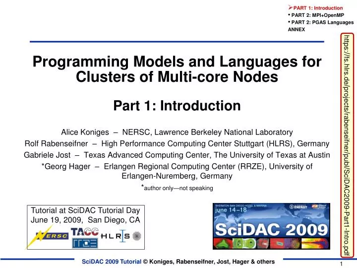
Programming Models and Languages for Clusters of Multi-core Nodes Part 1: Introduction. Alice Koniges – NERSC, Lawrence Berkeley National Laboratory Rolf Rabenseifner – High Performance Computing Center Stuttgart (HLRS), Germany

E N D
Programming Models and Languages for Clusters of Multi-core NodesPart 1: Introduction Alice Koniges – NERSC, Lawrence Berkeley National Laboratory Rolf Rabenseifner – High Performance Computing Center Stuttgart (HLRS), Germany Gabriele Jost – Texas Advanced Computing Center, The University of Texas at Austin *Georg Hager – Erlangen Regional Computing Center (RRZE), University of Erlangen-Nuremberg, Germany *author only—not speaking Tutorial at SciDAC Tutorial DayJune 19, 2009, San Diego, CA • PART 1: Introduction • PART 2: MPI+OpenMP • PART 2: PGAS Languages • ANNEX https://fs.hlrs.de/projects/rabenseifner/publ/SciDAC2009-Part1-Intro.pdf 05/19/09, Author: Rolf Rabenseifner
Mulitcore is coming, so we are considering models beyond MPI everywhere • Mixed or Hybrid (OpenMP + MPI) • PGAS languages We will examine performance of Hybrid, And give and introduction to PGAS First, a quick overview of architectures… https://fs.hlrs.de/projects/rabenseifner/publ/SciDAC2009-Part1-Intro.pdf
Some of the “top 10” systems www.top500.org: Nov 2008 #1 Petaflop Record LANL Roadrunner Rmax: 1.105 Pflops 129600 Cores CRAY XT4, 5 XT5 Jaguar #2 ORNL/NCCS 150152 CoresRmax: 1.059 Pflops XT4 Franklin # 7 LBNL/NERSC NASA/Ames Pleiades #3 SGI Altix ICE 8200 51200 Cores Rmax: 487 Tflops • 499 (498) scalar, 1 (2) vector • MPPs 88 (98) • Clusters 410 (400) in majority • Constellations 2 (2) • invoked to distinguish • “clusters of large SMP nodes” • #Procs/#Nodes ≥ #Nodes • () denotes previous year June list Texas “Ranger” #6 U. Texas 26544 Proc Rmax: 326 Tflops IBM Blue Gene(L,P) Systems #4, 5 LLNL (L): Rmax: 478 Tflops Argonne National Lab (P): 450 Tflops Section Header without an outline-slide: Recent Computer Center Choices and Comparisons 185 IBM systems 210 HP systems 22 Cray systems 19 Dell systems 17 SGI systems
Multi-core orMulti-processor Cache-based Chip Typical Layout: • Each processor: • L1 caches • Registers • Functional units • Each chip (shared) • L2 cache • L3 cache • Path to memory CPU Core L1 CPU Core L1 CPU Core L1 CPU Core L1 L2 Cache L2 Cache L3 Fabric Controller Fabric Controller L3 Memory Controller L1 = level 1 L2 = level 2, etc. Memory Controller Memory Memory On a multi-core chip, get more computational power with (often) same bandwidth to memory, so need to be effective with cache reuse Note: Different access for L3 cache
Quad Cores and Beyond Example: Intel Dunnington 6 cores 16 MB shared L3 per socket CPU Core 1 L1, L2 CPU Core 2 L1,L2 CPU Core 3 L1, L2 CPU Core 4 L1, L2 L3 Cache common to all 4 Memory New many-core chips 64 and up are likely to be appearing in HPC Example: 4 core AMD Barcelona Quad Core systems now dominate the top500
The x86 multicore evolution P P P P P P P P C C C C C C P P P P C C C C Chipset C C C C C C C C Chipset Memory Memory P P P P P P P P C C C C C C C C C C C C C C C C C C MI MI P P P P P P Memory Memory C C C C C C C C C Chipset L3 Cache Memory Intel 4-way „Dunnington“ Hexcore system Woodcrest „Core2Duo“ Intel HPC Compute node evolution Clovertown / Harpertown„Core2Quad“ Nehalem „Core i7“ 1.9 Billion transistors On-chip cache hierarchy
Current Multicore SMP Systems can have different memory access and cache use patterns Intel Clovertown AMD Opteron Core2 Core2 Core2 Core2 Core2 Core2 Core2 Core2 Opteron Opteron Opteron Opteron 4GB/s (each direction) 4MB Shared L2 4MB Shared L2 4MB Shared L2 4MB Shared L2 1MB victim 1MB victim 1MB victim 1MB victim HT HT SRI / crossbar SRI / crossbar Front Side Bus FSB 10.6 GB/s 10.6 GB/s 128b memory controller 128b memory controller Chipset (4x64b controllers) 10.66 GB/s 10.66 GB/s 21.3 GB/s(read) 10.6 GB/s(write) 667MHz DDR2 DIMMs 667MHz DDR2 DIMMs 667MHz FBDIMMs Non-uniform Memory Access Uniform Memory Access Adapted from Sam Williams, John Shalf, LBL/NERSC et al.
A typical IBM Power SeriesLLNL’s “Purple” • Purple System Specs • 93.4 TF/s peak from 12,288 Power5 @ 1.9 GHz • 50 TB memory • 1,536 8-way SMP nodes • 32 GB memory • 8x1.9 GHz Power5 single core ASIC • Blue Waters POWER7 • Timescale ~2011 • > 200,000 cores • Private L1 and L2 caches for each core, shared L3 • NSF machine sited at U. Illinois Possible Chip Configuration: • 8 cores per chip arranged in dual-chip modules • 4 hardware threads per core
Node Card (32 chips 4x4x2) 32 compute, 0-1 IO cards Blue Gene/P System 72 Racks Cabled 8x8x16 Rack 32 Node Cards 1024 chips, 4096 procs 1 PF/s 144 TB 14 TF/s 2 TB Compute Card 1 chip, 20 DRAMs 435 GF/s 64 GB Chip 4 processors 13.6 GF/s 2.0 (or 4.0) GB DDR Supports 4-way SMP 13.6 GF/s 8 MB EDRAM By permission kjordan@us.ibm.com
OpenMP MPI combination was not available on BG/L, but now is with SMP mode on BG/P BG/L Mode 1 (Co-processor mode - CPM): • CPU0 does all the computations • CPU1 does the communications • Communication overlap with computation • Peak comp perf is 5.6/2 = 2.8 GFlops BG/L Mode 2 (Virtual node mode - VNM): • CPU0, CPU1 independent “virtual tasks” • Each does own computation and communication • The two CPU’s talk via memory buffers • Computation and communication cannot overlap • Peak compute performance is 5.6 Gflops BG/P Virtual Node Mode, SMP Mode, Dual Mode CPU0 CPU1 CPU0 CPU1 Virtual Node Mode SMP Mode Dual Mode CPU 0 Rank 0 CPU 1 Rank 1 CPU 0 Rank 0 CPU 1 thread CPU 0 Rank 0 CPU 1 thread BG/P Figure courtesy K. Jordon, IBM CPU 2 Rank 2 CPU 3 Rank 3 CPU 2 thread CPU 3 thread CPU 2 Rank 1 CPU 3 thread
Franklin: NERSC’s Cray XT4 • System structure • 9,660 nodes • originally 19,320 cores, recently upgraded to 38,640 • Interconnect: Cray SeaStar2, 3D Torus >6 TB/s Bisection Bandwidth; >7 GB/s Link Bandwidth • Shared Disk: 400+ TBs • Performance: • Sustained application performance: 38 Tflops • Peak performance: 355 Tflops • Linpack: 266 Tflops
Mix-and-match to meet workload requirements CRAY Cray XT4 Optimized for compute/interconnect balance Cray XT5 Optimized for memory-intensive and/or compute-biased workloads 4-way SMP Node Cray X2 Blade high bandwidth memory intensive >25GFLOPs/single core vector based CPU and global address space scaling to 32K processors XT5h diagrams courtesy John Levesque, CRAY Slide 12 10/28/2014
AMD Opteron Processor 16 instruction bytes fetched per cycle L2 Cache 1 MB 16-way assoc L1 InstructionCache 64KB Fetch Branch Prediction Scan/Align Microcode Engine Fastpath L1 DataCache 64KB 2-way assoc mOPs Bus Unit Instruction Control Unit (72 entries) System Request Queue Int Decode & Rename FP Decode & Rename Crossbar 44-entry Load/Store Queue Res Res Res 36-entry FP scheduler Memory Controller AGU AGU AGU FADD FMUL FMISC ALU ALU ALU HyperTransportTM MULT 9-way Out-Of-Order execution Courtesy John Levesque • 36 entry FPU instruction scheduler • 64-bit/80-bit FP Realized throughput (1 Mul + 1 Add)/cycle: 1.9 FLOPs/cycle • 32-bit FP Realized throughput (2 Mul + 2 Add)/cycle: 3.4+ FLOPs/cycle
Simplified memory hierachy on the AMD Opteron registers 16 SSE2 128-bit registers 16 64 bit registers 2 x 8 Bytes per clock, i.e. Either 2 loads, 1 load 1 store, or 2 stores (38 GB/s on 2.4 Ghz) • 64 Byte cache line • complete data cache lines are loaded from main memory, if not in L2 cache • if L1 data cache needs to be refilled, then storing back to L2 cache • 64 Byte cache line • write back cache: data offloaded from L1 data cache are stored here first until they are flushed out to main memory L1 data cache 8 Bytes per clock L2 cache …... 16 Bytes wide data bus => 6.4 GB/s for DDR400 Main memory Courtesy John Levesque
SSE vectorization is available on AMD • Function in-lining • Enable SSE vectorization (when available) - streaming SIMD extensions • Fine-grained data parallelism • Check compiler output for vectorization of loops • C and C++ codes can inhibit vectorization 128 a(0) a(1) + b(0) b(1) SIMD is single instruction multiple data
x86 Architecture:SIMD Operations • Possible data types in an SSE register 16x 8bit 8x 16bit 4x 32bit integer 2x 64bit 1x 128bit 4x 32 bit floating point 2x 64 bit
x86 Architecture:Floating Point Operations and SIMD xmm0 x3 x2 x1 x0 y3 y2 y1 y0 xmm1 + + + + x3 + y3 x2 + y2 x1 + y1 x0 + y0 xmm1 • Example: Single precision FP packed vector addition • Four single precision FP additions are done in one single instruction • Intel Core2: 3/5-cycle latency & 1/1-cycle throughput for double precision SSE2 ADD/MULT leading to a peak performance of 4 (DP) FLOPs/cycle • Single precision: 8 SP FLOPs/cycle • AMD64/K10 (2008): same characteristics
Sun Constellation Linux Cluster “Ranger”Texas Advanced Computing Center • First of the new NSF Track2 HPC • Number 3 on the Top 500 list for June 2008 • 3936 Nodes, 62,976 Cores • Peak Performance 579.4 Tflops • 15,744 Quad-Core AMD Opteron at 2.3 GHz
Cell Processor--was enhanced for HPC S P U S P U S P U S P U 64b Power Processor Mem. Contr. P P U R R AC M I C B I C Synergistic Processor MIB Config. IO S P U S P U S P U S P U Synergistic Processor Think of the typical cell processor designed for the PlayStation PS3: CPU Calculation power is ~220 - 230 Gflops (Cell single precision)* GPU Calculation power is ~1.8 TFlops (Nvidia graphics chip) Total System Calculation power is 2 TFlops *Cell has nominally 8 SPE’s, this is 4GHz estimate, PS3 designed to use 7 of these. Each SPE is capable of sustaining 4 FMADD per cycle Cell Processor courtesy Doug Joseph, IBM
TensilicaDP PPC450 New Designs for Power Efficiency, High Parallelism/Concurrency) Green Flash Project approach at LBL uses low-power embedded Tensilica Processors • Power5 (Server) • 389 mm2 • 120 W @ 1900 MHz • Intel Core2 sc (Laptop) • 130 mm2 • 15 W @ 1000 MHz • PowerPC450 (BlueGene/P) • 8 mm2 • 3 W @ 850 MHz • Tensilica DP (cell phones –and Green Flash energy-efficient architectures) • 0.8 mm2 • 0.09 W @ 650 MHz Intel Core2 (laptop) Power 5 (ASCI Purple) Even if each core operates at 1/3 to 1/10th efficiency of largest chip, you can pack 100s more cores onto a chip and consume 1/20 the power! Green Flash: Wehner. Oliker, and Shalf (LBL) Rowen (Tensillca)
An 80-tile 1.28 TFLOPS INTEL CPU Prototype Diagrams courtesy of Intel Tiles arranged in 10 X 8 2D mesh
Note on the Hands-on Examples:The Poisson Problem • Simple elliptic partial differential equation • Occurs in many physical problems • Fluid flow, electrostatics, equilibrium heat flow • Many algorithms for solution • This illustrates a sub-optimal one, that it is easy to understand and is typical of a data-parallel algorithm • Available in your .tar distribution in various languages
Jacobi Iteration (Fortran Ordering) Process 0 Process 1 Process 2 Process 3 Boundary Point Interior Node • Simple parallel data structure • Processes exchange columns with neighbors • Local part declared as xlocal(m,0:n+1)
Shekhar Borkar, Intel Kirk Jordan, IBM John Levesque, CRAY Charles Grassl, IBM/Instrumental John Shalf, Sam Williams, Kathy Yelick LBL Ken Koch, Andy White LANL Thanks! – Additional Slide Contributions Thanks! – NERSC Hands-On and Codes: • NERSC Consulting Group • NERSC Systems Groups • NERSC Accounts and Managers granting access • Berkeley UPC Group • Especially: Woo-Sun Yang, Helen He, Katie Antypas, Yili Zheng, Cary Whitney, Verrill Rinehart, Nicholas Cardo, Francesca Verdier, Howard Walter, David Skinner, Clayton Bagwell https://fs.hlrs.de/projects/rabenseifner/publ/SciDAC2009-Part1-Intro.pdf