Download
1 / 12
140 likes | 280 Vues
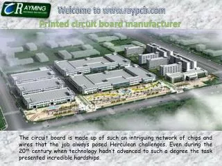
Printed circuit board manufacturing.

E N D
Printed circuit board manufacturing A printed circuit board, or PCB, is used to mechanically support and electrically connect electronic components using conductive pathways, tracks or signal traces etched from copper sheets laminated onto a non-conductive substrate. It is also referred to as printed wiring board (PWB) or etched wiring board. A PCB populated with electronic components is a printed circuit assembly (PCA), also known as a printed circuit board assembly (PCBA). Printed circuit boards are used in virtually all but the simplest commercially-produced electronic devices. PCBs are inexpensive, and can be highly reliable. They require much more layout effort and higher initial cost than either wire wrap or point-to-point construction, but are much cheaper and faster for high-volume production; the production and soldering of PCBs can be done by totally automated equipment. Much of the electronics industry's PCB design, assembly, and quality control needs are set by standards that are published by the IPC organization (the Association of Connecting Electronics Industries). Materials Conducting layers are typically made of thin copper foil. Insulating layers are typically laminated together with epoxy resin (pre-impregnated). The board is typically coated with a solder mask that is green in color. Other colors that are normally available are blue, black, white and red.
There are quite a few different dielectrics that can be chosen to provide different insulating values depending on the requirements of the circuit.Some of these dielectrics are Teflon, FR-4, FR-1, CEM-1 or CEM-3. Well known prepreg materials used in the PCB industry are FR-2 (Phenolic cotton paper), FR-3 (Cotton paper and epoxy), FR-4 (Woven glass and epoxy), FR-5 (Woven glass and epoxy), FR-6 (Matte glass and polyester), G-10 (Woven glass and epoxy), CEM-1 (Cotton paper and epoxy), CEM-2 (Cotton paper Fig.13.1. Pre-coated photoresist fibreglass (FR4) board and epoxy), CEM-3 (Woven glass and epoxy), CEM-4 (Woven glass and epoxy), CEM-5 (Woven glass and polyester). Thermal expansion is an important consideration especially with BGA and naked die technologies, and glass fiber offers the best dimensional stability. FR-4 is by far the most common material used today. The board with copper on it is called "copper-clad laminate“. Copper foil thickness can be specified in micrometers. Patterning (etching) The vast majority of printed circuit boards are made by bonding a layer of copper over the entire substrate, sometimes on both sides, (creating a "blank PCB") then removing unwanted copper after applying a temporary mask (e.g. by etching), leaving only the desired copper traces. A few PCBs are made by adding traces to the bare substrate (or a substrate with a very thin layer of copper) usually by a complex process of multiple electroplating steps. The PCB manufacturing
method primarily depends on whether it is for production volume or sample/prototype quantities. • Silk screen printing – the main commercial method. • Photographic methods–used when fine line widths are required. • There are three common "subtractive" methods Fig.13.2. • (methods that remove copper) used for the production of printed circuit boards: • Silk screen printing uses etch-resistant inks to protect the copper foil. Subsequent etching removes the unwanted copper. Alternatively, the ink may be conductive, printed on a blank (non-conductive) board. The latter technique is also used in the manufacture of hybrid circuit board. A hybrid integrated circuit, HIC, hybrid microcircuit, or simply hybrid is a miniaturized electronic circuit constructed of individual devices, such as semiconductor devices (e.g. transistors and diodes) and passive components (e.g. resistors, inductors, transformers, and capacitors), bonded to a substrate or PCB. Hybrid circuits are often encapsulated in epoxy. • Photoengraving uses a photomask and developer to selectively remove a photoresist coating. The remaining photoresist protects the copper foil. Subsequent etching removes the unwanted copper. The photomask is usually prepared with a photo plotter from data produced by a technician using, or computer-aiding manufacturing (CAM) software. Laser-printed transparencies are typically employed for photo tools; however, direct laser imaging techniques are
being employed to replace phototools for high-resolution requirements. PCB milling uses a two or three-axis mechanical milling system to mill away the copper foil from the substrate. A PCB milling machine (referred to as a 'PCB Prototyper') operates in a similar way to a plotter, receiving commands from the host software that control the position of the milling head in the x, y, and (if relevant) z axis. Data to drive the Prototyper is extracted from files generated in PCB design software and stored in Gerber file format. The Gerber format is a file format used by PCB industry software to describe the images of a printed circuit board (copper layers, solder mask, legend, etc.) as well as the drilling and milling data. The Gerber format is the de-facto industry standard for printed circuit board image transfer. Multi-layer printed circuit boards With the complexity of electronic circuits increasing, it is not always possible to provide all the connectivity that is required using just the two sides of the PCB. This occurs quite commonly when dense microprocessor and other similar boards are being designed. When this is the case multilayer boards are required. Fig.13.3. Printer to manufacture conductive traces
The manufacture of multi-layer printed circuit boards, although it uses the same processes as for single layer boards, requires a considerably greater degree of accuracy and manufacturing process control.The boards are made by using much thinner individual boards, one for each layer, and these are then bonded together to produce the overall PCB. As the number of layers increases, so the individual boards must become thinner to prevent the finished PCB from becoming too thick. Additionally the registration between the layers must be very accurate to ensure that any holes line up. To bond the different layers together the board is heated to cure the bonding material. This can lead to some problems of deformation (warp). Large multi-layer boards can have a distinct warp on them if they are not designed correctly. PCB holes and vias Holes, often called via holes or vias are needed within a PCB to connect the different layers together at different points. Holes may also be needed to enable leaded components to be mounted on the PCB. Additionally some fixing holes may be needed. Normally the inner surfaces of the holes have copper layer so that they electrically connect the layers of the board. These "plated through holes" are produced using a plating process. In this way the layers of the board can be connected.
Drilling is then accomplished using numerically controlled drilling machines, the data being supplied from the PCB CAD design software. It is worth noting that reducing the number of different sizes of holes can help reduce the cost of the PCB manufacture. It may be necessary for some holes to only exist within the centre of the board, for example when inner layers of the board need to be connected. These "blind vias" are drilled in the relevant layers prior to the PCB layers being bonded together. PCB solder plating and solder resist When a PCB is soldered it is necessary to keep the areas that are not to be soldered protected by a layer of what is termed solder resist. The addition of this layer helps prevent unwanted short circuits on the PCB boards caused by the solder. The solder resist normally consists of a Fig.13.4. A PCB as a design on a computer (left) and realized as a board assembly populated with components (right). polymer layer and protects the board from solder and other contaminants. The colour of the solder resist is normally deep green or red. In order to enable the components added to the board, either leaded or SMT to solder to the board easily, exposed areas of the board are normally "tinned" or plated with solder. Occasionally boards, or areas of boards may be gold plated. This may be applicable if some copper fingers are to be used for edge connections.
As the gold will not tarnish, and it offers good conductivity it provides a good connection at a low cost. Solder Plating | Solder Resist Pads and lands which will require components to be mounted on are plated to allow solderability of the components. Bare copper is not readily solderable and requires the surface to be plated with a material that facilitates soldering. In the past a lead based tin was used to plate the surfaces, but with RoHS compliance enacted newer materials are being used such as nickel and gold to both offer solderability and comply with RoHS standards. Areas that should not be solderable are covered with a material to resist soldering. Solder resist refers a polymer coating that acts as a mask and prevents solder from bridging traces and possibly creating short circuits to nearby component leads.
The process of automatized manufacture of the PCBA Fig.13.5 PCB uploading systemglass fibre based board known as FR4.
The reflow profiles are based on experiences to ensure that all packages can be successfully and reliably assembled. The figure bellow shows the range of temperature profiles and the table 1 lists the reflow parameters and peak temperatures. Table 13.1. Lead-free reflow profile Fig. 13.6. Convection reflow profile