Download
1 / 55
560 likes | 676 Vues
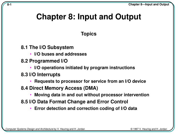
Chapter 8: Input and Output. Topics. 8.1 The I/O Subsystem I/O buses and addresses 8.2 Programmed I/O I/O operations initiated by program instructions 8.3 I/O Interrupts Requests to processor for service from an I/O device 8.4 Direct Memory Access (DMA)

E N D
Chapter 8: Input and Output Topics 8.1 The I/O Subsystem • I/O buses and addresses 8.2 Programmed I/O • I/O operations initiated by program instructions 8.3 I/O Interrupts • Requests to processor for service from an I/O device 8.4 Direct Memory Access (DMA) • Moving data in and out without processor intervention 8.5 I/O Data Format Change and Error Control • Error detection and correction coding of I/O data
Memory Subsystem Input/Output Subsystem CPU Components of a Computer System • I/O subsystem connects CPU to external devices other than memory • Keyboard, mouse, network, monitor, other peripherals • Disk drives • These devices have very different characteristics • Interface protocol • Timing - 100’s to millions of clock cycles
Three Requirements of I/O Data Transmission (1) Data location • Correct device must be selected • Data must be addressed within that device (2) Data transfer • Amount of data varies with device and may need be specified • Transmission rate varies greatly with device • Data may be output, input, or either with a given device (3) Synchronization • For an output device, data must be sent only when the device is ready to receive it • For an input device, the processor can read data only when it is available from the device
Location of I/O Data • Data location may be trivial once the device is determined • Character from a keyboard • Character out to a serial printer • Location may involve searching • Record number on a tape drive • Track seek and rotation to sector on a disk • Location may not be simple binary number • Drive, platter, track, sector, word on a disk cluster
Synchronization—I/O Devices Are Not Timed by Master Clock • Not only can I/O rates differ greatly from processor speed, but I/O is asynchronous • Processor will interrogate state of device and transfer information at clock ticks • I/O status and information must be stable at the clock tick when it is accessed • Processor must know when output device can accept new data • Processor must know when input device is ready to supply new data
( a ) S y n c h r o n o u s i n p u t ( b ) S e m i s y n c h r o n o u s i n p u t R e a d y ( M ) A c k n o w l e d g e ( S ) v a l i d D a t a ( S ) S t r o b e d a t a ( M ) ( c ) A s y n c h r o n o u s i n p u t Interfacing to Asynchronous Devices Fig 8.7 Synchronous, Semi-synchronous, and Asynchronous Data Input C y c l e t i m e C y c l e t i m e o f m a s t e r o f m a s t e r R e a d ( M ) R e a d ( M ) v a l i d v a l i d D a t a ( S ) D a t a ( S ) S t r o b e d a t a ( M ) C o m p l e t e ( M ) S t r o b e d a t a ( M ) • Used for memory to CPU read with few cycle memory • Used for register to register inside CPU • Used for I/O over longer distances (feet)
Fig 8.7c Asynchronous Data Input Yes, you may. You’re welcome. May I? Thanks. Ready Acknowledge v a l i d Data Strobe data
Reducing Location and Synchronization to Data Transfer • Since the structure of device data location is device dependent, device should interpret it • The device must be selected by the processor, but • Location within the device is just information passed to the device • Synchronization can be done by the processor reading device status bits • Data available signal from input device • Ready to accept output data from output device • Speed requirements will require us to use other forms of synchronization: discussed later • Interrupts and DMA are examples
M e m o r y b u s M e m o r y b u s M e m o r y b u s C o n t r o l C o n t r o l M e m o r y c o n t r o l A d d r e s s A d d r e s s A d d r e s s C P U M e m o r y C P U M e m o r y C P U M e m o r y D a t a D a t a D a t a A d d r e s s I / O I / O I / O D a t a s y s t e m s y s t e m s y s t e m I / O c o n t r o l I / O c o n t r o l C o n t r o l I / O b u s ( a ) S e p a r a t e m e m o r y a n d I / O b u s e s ( b ) S h a r e d a d d r e s s a n d d a t a l i n e s ( c ) S h a r e d a d d r e s s , d a t a , a n d c o n t r o l ( i s o l a t e d I / O ) l i n e s ( m e m o r y - m a p p e d I / O ) Fig 8.2 Independent and Shared Memory and I/O Buses • Allows tailoring bus to its purpose, but • Requires many connections to CPU (pins) • Memory and I/O access can be distinguished • Timing and synchronization can be different for each • Least expensive option • Speed penalty
Programmed I/O • CPU directly manages the I/O process through program control • I/O device is controlled by reading and writing information into device interface registers (inside I/O device) • I/O device interface registers are configured to look like additional memory locations (memory mapped I/O) • Combine memory control and I/O control lines to make one unified bus for memory and I/O • Reduces the number of connections to the processor chip • Increased generality may require a few more control signals • Standardizes data transfer to and from the processor • Asynchronous operation is optional with memory, but demanded by I/O devices
M e m o r y c e l l s : a l l i n o n e m a i n m e m o r y s u b u n i t A d d r e s s s p a c e I / O r e g i s t e r s : d i s t r i b u t e d a m o n g m a n y I / O d e v i c e s , n o t a l l u s e d Fig 8.3 Address Space of a Computer Using Memory-Mapped I/O . . .
Programmed I/O - More Details • Requirements for a device using programmed I/O • Device operations take many instruction times • One word data transfers—no burst data transmission • Program instructions have time to test device status bits, write control bits, and read or write data at the required device speed • Example status bits: • Input data ready • Output device busy or off-line • Example control bits: • Reset device • Start read or start write
Fig 8.4 Programmed I/O Device Interface Structure M e m o r y b u s C o n t r o l A d d r e s s • Focus on the interface between the unified I/O and memory bus and an arbitrary device. Several device registers (memory addresses) share address decode and control logic. C P U D a t a A d d r e s s d e c o d e r s I / O i n t e r f a c e I / O i n t e r f a c e I / O i n t e r f a c e I n O u t C o m m a n d S t a t u s P r i n t e r K e y b o a r d D i s k d r i v e D e v i c e i n t e r f a c e r e g i s t e r s I / O d e v i c e
Programmed I/O Example - An FP Coprocessor for the SRC • A floating point (FP) coprocessor that can multiply two 32-bit FP numbers and return the result to the SRC • The coprocessor is memory mapped and uses 4 device registers mapped to 4 memory locations in the SRC’s memory space • The first two registers are write only and are used to hold the two FP operands to be multiplied • The third register is read-write and is the status register • A write (of any data value) to this register starts the multiply operation • A read from this register returns a non-zero value if the coprocessor is busy - the current calculation is not complete • The fourth register is read only and holds the result of the FP multiply operation • A read to this register before the result is computed causes wait states to be inserted until the operation is complete
Programmed I/O Example (cont.) • There are two basic modes of operation for this coprocessor: • Wait for completion 1) Write FP operands to A and B registers 2) Write (any data) to status register to start multiply operation 3) Read from result register - wait states inserted until operation is complete • Polling 1) Write FP operands to A and B registers 2) Write (any data) to status register to start multiply operation 3) Read from status register to check busy (non-zero value is returned) 4) If busy, repeat step 3 until not busy (zero value is returned) 5) Read from result register - no wait states will be inserted
Example SRC Computer System Memory Map Address 0x00000000 ROM address space organized as 8K x 32 bit words 0x00007FFF 0x00008000 RAM address space organized 2K x 32 bit words 0x00009FFF FP coprocessor A operand register 0x0000A000 FP coprocessor B operand register 0x0000A001 FP coprocessor registers (4) FP coprocessor Status register 0x0000A002 FP coprocessor Result register 0x0000A003 0x0000A004 Unused 0x0000AFFF Programmed I/O Example - Memory Map • FP coprocessor device registers are placed in SRC memory map above system ROM and RAM
Programmed I/O ExampleSystem Architecture Memory Controller SRC CPU System ROM System RAM FP Coprocessor Controller FP Coprocessor
Programmed I/O ExampleSystem Architecture (cont.) FP Coprocessor Controller FP Coprocessor
Programmed I/O ExampleFP coprocessor Address Decoding • FP coprocessor selected for any address in the range of 0x0000A000
Programmed I/O - Code Example • Polling - the CPU reads the status register in a loop to determine when the operation is complete • This would allow the CPU to potentially do other things while it is waiting (interrupts) .org 0 ; 0x1000 ld r1, data1 ; Load multiplier from RAM ld r2, data2 ; Load multiplicand from RAM lar r30, loop ; load address for loop st r1, a_fp_data ; send A to fp coprocessor st r2, b_fp_data ; send B to fp coprocessor st r3, status ; start fp coprocessor loop: ld r3, status ; load status to check for busy brnz r30,r3 ; loop while status = busy (!= 0) ld r4, fp_result ; load result back from fp coprocessor st r4, Result ; store result in RAM stop .org 32768 ; 0x8000 - start of RAM data1: .dw 1 ; storage for result data2: .dw 1 ; storage for result Result: .dw 1 ; storage for result .org 40960 ; 0xA000 - start address for FP coprocessor a_fp_data: .dw 1 ; location for A data b_fp_data: .dw 1 ; location for B data status: .dw 1 ; location for status fp_result: .dw 1 ; location for FP result
Programmed I/O - Code Example • Wait - the CPU reads the result register and wait states are inserted until the result is ready • The CPU is blocked until the result is returned .org 0 ; 0x1000 ld r1, data1 ; Load multiplier from RAM ld r2, data2 ; Load multiplicand from RAM st r1, a_fp_data ; send A to fp coprocessor st r2, b_fp_data ; send B to fp coprocessor st r3, status ; start fp coprocessor ld r4, fp_result ; load result back from fp coprocessor (wait) st r4, Result ; store result in RAM stop .org 32768 ; 0x8000 - start of RAM data1: .dw 1 ; storage for result data2: .dw 1 ; storage for result Result: .dw 1 ; storage for result .org 40960 ; 0xA000 - start address for FP coprocessor a_fp_data: .dw 1 ; location for A data b_fp_data: .dw 1 ; location for B data status: .dw 1 ; location for status fp_result: .dw 1 ; location for FP result
I/O Interrupts • Key idea: instead of processor executing wait loop, device requests interrupt when ready • Interrupt line is another (asynchronous) input to CPU • The interrupting device typically must return the vector address and interrupt information bits • Processor must tell device when to send this information—done by acknowledge signal • Request and acknowledge form a communication handshake pair • CPU must have the capacity to disable interrupts • Critical portions of the code may require completion without being interrupted for correct operation • It should be possible to disable interrupts from individual devices
Interrupts - The Basic Process • CPU is executing some normal code • I/O device becomes ready for servicing (e.g., user hits a key, network traffic arrives, etc.) • I/O device requests interrupt to indicate to CPU that it needs service - asserts IREQ line • CPU acknowledges interrupt request - asserts IACK line • I/O device sends data to CPU to indicate which device it is and possibly what type of service it needs - interrupt vector • CPU selects code to execute to provide I/O device with requested service - interrupt service routine • CPU returns to execution of normal code before interrupt
I/O Device 0 I/O Device 1 I/O Device 2 I/O Device 3 Interrupt Requests CPU IREQ Interrupt flip-flop Single Line Interrupt System
I/O Device 0 I/O Device 1 I/O Device 2 I/O Device 3 Interrupt Requests (cont.) CPU IREQ0 IREQ1 Interrupt register IREQ2 IREQ3 Multiple Line Interrupt System
I/O Device 0 I/O Device 1 I/O Device 2 I/O Device 3 Acknowledging Interrupts IREQ0 CPU IREQ1 IREQ2 IREQ3 IACK3 IACK2 IACK1 IACK0 Multiple Line Interrupt Acknowledgment
I / O b u s d a t a i r e q i a c k I / O d e v i c e I / O d e v i c e I / O d e v i c e 0 1 j Acknowledging Interrupts (cont.) CPU Daisy-Chained Interrupt Acknowledgement Signal
Disabling and Enabling Interrupts • CPU should have some method of disabling interrupts during critical portions of the code • Operating system functions • Interrupt service routines • The normal method is to have an interrupt mask bit which when 0, prevents the CPU’s control unit from seeing the interrupt • The CPU then has instruction for enabling or disabling interrupts (setting or clearing this mask bit) eni ; enable interrupts dsi ; disable interrupts CPU Interrupt mask bit Enable/Disable interrupts signal from control unit Q D IREQ Interrupt signal to control unit Interrupt signal from I/O devices
Servicing Interrupts • Code location for interrupt service routine may be “hardwired” - (single I/O device or multiple line interrupt system) • More likely is that the I/O device provides the location of the interrupt service routine to the CPU - Interrupt Vector • I/O device places interrupt vector onto the CPU’s data bus • Vector may contain address of service routine AND information on type of service needed CPU Data Bus IREQ IACK I/O Device 0
Servicing Interrupts - Typical Timing I/O Device signals interrupt to CPU I/O Device signals CPU that interrupt vector is valid IREQ CPU signals I/O Device it is ready to service interrupt CPU signals I/O Device that it has received the vector IACK Interrupt vector from I/O device to CPU DATA
I n t e r r u p t I n t e r r u p t r e q u e s t e n a b l e d a t a 2 3 . . 1 6 v e c t 7 . . 0 D Q D Q d a t a 1 5 . . 0 i n f o 1 5 . . 0 Q Q i r e q o . c . i a c k Fig 8.12 Simplified Interrupt Circuit for an I/O Interface • Request and enable flags per device • Returns vector and interrupt information on bus when acknowledged
Interrupt Service Routine • Interrupt service routine actually performs the work required by the I/O device • Storing the block of data from the disk into memory • Storing the value of the key pressed by the user in a register • Writing the value of the next character to the network transmitter • The interrupt service routine functions like a subroutine call • The fact that the routine executed must be invisible to the normal program that was running when the interrupt occurred - contents of any registers used by the interrupt service routine must be saved and restored • The interrupt service routine must return control to the program that was executing at the same point where it stopped and the interrupt service routine started
Saving Processor State - The Stack • Most processors include a stack to simplify saving and restoring the contents of registers that must be used during an interrupt service routine (also useful in normal subroutine calls) • There is a special register called a stack pointer that is used to address memory during register saves and restores • Memory is addressed via register indirect addressing using the stack pointer as the address register • The programmer must initialize the stack pointer to a portion of RAM reserved for the stack data • The stack behaves as a last-in, first-out (LIFO) queue • Stack manipulation instructions (example) las c2(rb) ;load stack pointer with displacement address lds c2(rb) ;load stack pointer from displacement address sts c2(rb) ;store stack pointer to displacement address push ra ;store register ra on stack, increment stack pointer pop ra ;load register ra on stack, decrement stack pointer
R0 R1 R2 R(N-1) Stack Operation Example las #32678 ;load stack pointer with 0x8000 push r0 ;store r1 on stack push r1 ;store r2 on stack push r2 ... ;some code for service routine ... ;which uses registers r0,r1, and r2 pop r2 ;restore r2 from stack pop r1 ;restore r1 from stack pop r0 ;restore r0 from stack Memory Subsystem RAM memory Address CPU 0x8000 R0 R1 R2 SP
General Functions of an Interrupt Handler (1) Save the state of the interrupted program (using stack) (2) Do programmed I/O operations to satisfy the interrupt request (3) Restart or turn off the interrupting device (4) Restore the state and return to the interrupted program
Nested Interrupts—Interrupting an Interrupt Handler • Some high-speed devices have a deadline for interrupt response • Longer response times may miss data on a moving medium • A real-time control system might fail to meet specifications • To meet a short deadline, it may be necessary to interrupt the handler for a slow device • The higher priority interrupt will be completely processed before returning to the interrupted handler • Hence the designation nested interrupts • Interrupting devices are priority ordered by shortness of their deadlines
Steps in the Response of a Nested Interrupt Handler (1) Save the state changed by interrupt (IPC and II); (2) Disable lower priority interrupts; (3) Re-enable exception processing; (4) Service interrupting device; (5) Disable exception processing; (6) Re-enable lower priority interrupts; (7) Restore saved interrupt state (IPC and II); (8) Return to interrupted program and re-enable exceptions.
Direct Memory Access (DMA) • Allows external I/O devices to access memory without processor intervention • Requires a DMA interface device • Must be “set up” or programmed and transfer initiated DMA Example: • CPU needs a block of data from the disk • CPU tells disk DMA controller where data is on disk and where data should be placed in memory • CPU goes on and does “other things” • Disk DMA controller fetches data from disk into buffer (inside controller) • Disk DMA controller transfers data from buffer directly into memory (cycle stealing) • Disk DMA controller informs CPU (via interrupt) that transfer is complete and data is ready Disk Memory CPU Disk Controller (DMA) Disk data
Steps a DMA Device Interface Must Take to Transfer a Block of Data 1. Become bus master 2. Send memory address and R/W signal 3. Synchronized sending and receiving of data using Complete signal 4. Release bus as needed (perhaps after each transfer) 5. Advance memory address to point to next data item 6. Count number of items transferred and check for end of data block 7. Repeat if more data to be transferred
a d d r e s s I / O a d d r e s s d e c o d e M e m o r y a d d r e s s C o u n t R e a d , W r i t e C o n t r o l C o m p l e t e B u s c o n t r o l B u s r e q u e s t D e v i c e D M A c o n t r o l B u s g r a n t s e q u e n c e r d a t a D e v i c e P a c k i n g , u n p a c k i n g , a n d b u f f e r i n g d a t a Fig 8.18 I/O Interface Architecture for a DMA Device
D M A s e l e c t o r A d d r e s s P r o c e s s o r D e v i c e D e v i c e C o u n t S 1 S 2 B u s D M A m u l t i p l e x e r A d d r e s s 1 M e m o r y C o u n t 1 A d d r e s s 2 C o u n t 2 D e v i c e D e v i c e M 1 M 2 Fig 8.19 Multiplexer and Selector DMA Channels
Error Detection and Correction • Bit-error rate, BER, is the probability that, when read, a given bit will be in error • BER is a statistical property • Especially important in I/O, where noise and signal integrity cannot be so easily controlled • 10-18 inside processor • 10-8 - 10-12 or worse in outside world • Many techniques • Parity check • SECDED encoding • CRC
Parity Checking • Add a parity bit to the word • Even parity: add a bit if needed to make number of bits even • Odd parity: add a bit if needed to make number of bits odd • Example: for word 10011010, to add odd parity bit: 100110101
Hamming Codes • Hamming codes are a class of codes that use combinations of parity checks to both detect and correct errors. • They add a group of parity check bits to the data bits. • For ease of visualization, intersperse the parity bits within the data bits; reserve bit locations whose bit numbers are powers of 2 for the parity bits. Number the bits from l to r, starting at 1. • A given parity bit is computed from data bits whose bit numbers contain a 1 at the parity bit number.
C h e c k 2 C h e c k 1 C h e c k 0 B i t p o s i t i o n 1 2 3 4 5 6 7 P P D P D D D P a r i t y o r d a t a b i t 1 2 3 4 5 6 7 Fig 8.20 Multiple Parity Checks Making Up a Hamming Code • Add parity bits, Pi, to data bits, Di. • Reserve bit numbers that are a power of 2 for parity bits. • Example: P1 = 001, P2 = 010, P4 = 100, etc. • Each parity bit, Pi, is computed over those data bits that have a "1" at the bit number of the parity bit. • Example: P2 (010) is computed from D3 (011), D6 (110), D7 (111), ... • Thus each bit takes part in a different combination of parity checks. • When the word is checked, if only one bit is in error, all the parity bits that use it in their computation will be incorrect.
Example 8.1 Encode 1011 Using the Hamming Code and Odd Parity • Insert the data bits: P1 P2 1 P4 0 1 1 • P1 is computed from P1D3D5D7 = 1, so P1 = 1. • P2 is computed from P2D3D6D7 = 1, so P1 = 0. • P4 is computed from P1D5D6D7 = 1, so P1 = 1. • The final encoded number is 1 0 1 1 0 1 1. • Note that the Hamming encoding scheme assumes that at most one bit is in error.
SECDED (Single Error Correct, Double Error Detect) • Add another parity bit, at position 0, which is computed to make the parity over all bits, data and parity, even or odd. • If one bit is in error, a unique set of Hamming checks will fail, and the overall parity will also be wrong. • Let ci be true if check i fails, otherwise true. • In the case of a 1-bit error, the string ck-1, . . ., c1, c0 will be the binary index of the erroneous bit. • For example, if the ci string is 0110, then bit at position 6 is in error. • If two bits are in error, one or more Hamming checks will fail, but the overall parity will be correct. • Thus the failure of one or more Hamming checks, coupled with correct overall parity, means that 2 bits are in error. • This assumes that the probability of 3 or more bits being in error is negligible.
Example 8.2 Compute the Odd Parity SECDED Encoding of the 8-bit value 01101011 The 8 data bits 01101011 would have 5 parity bits added to them to make the 13-bit value P0 P1 P2 0 P4 1 1 0 P8 1 0 1 1. Now P1 = 0, P2 = 1, P4 = 0, and P8 = 0, and we can compute that P0, overall parity, = 1, giving the encoded value: 1 0 1 0 0 1 1 0 0 1 0 1 1