Download
1 / 2
20 likes | 106 Vues
Materials World Network on III-V Bismide Materials for IR and Mid IR Semiconductors Joanna M. Millunchick, University of Michigan Ann Arbor, DMR 0908745.

E N D
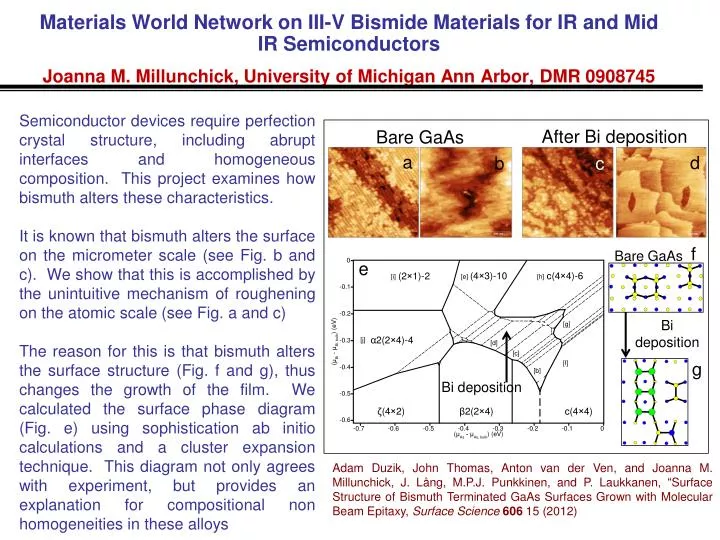
Materials World Network on III-V Bismide Materials for IR and Mid IR Semiconductors Joanna M. Millunchick, University of Michigan Ann Arbor, DMR 0908745 Semiconductor devices require perfection crystal structure, including abrupt interfaces and homogeneous composition. This project examines how bismuth alters these characteristics. It is known that bismuth alters the surface on the micrometer scale (see Fig. b and c). We show that this is accomplished by the unintuitive mechanism of roughening on the atomic scale (see Fig. a and c) The reason for this is that bismuth alters the surface structure (Fig. f and g), thus changes the growth of the film. We calculated the surface phase diagram (Fig. e) using sophistication ab initio calculations and a cluster expansion technique. This diagram not only agrees with experiment, but provides an explanation for compositional non homogeneities in these alloys a After Bi deposition d Bare GaAs c b f Bare GaAs e Bi deposition g Bi deposition Adam Duzik, John Thomas, Anton van der Ven, and Joanna M. Millunchick, J. Lång, M.P.J. Punkkinen, and P. Laukkanen, “Surface Structure of Bismuth Terminated GaAs Surfaces Grown with Molecular Beam Epitaxy, Surface Science 606 15 (2012)
3rd International Workshop on Bi-containing SemiconductorsJoanna M. Millunchick, University of Michigan Ann Arbor, DMR 0908745 • 40 researchers from all over North America, Europe, and Asia converged on the University of Victoria in Victoria British Columbia July 15-18, 2012 for the 3rd International Workshop on Bi-containing Semiconductors. These workshops are the result of an NSF sponsored international collaboration. • Technical talks included topics on: • Bismuthide growth and bismuth incorporation strategies • Structural, electrical, and optical characterization • Theoretical studies of bismuthide semiconductor properties and device physics • Device fabrication and performance • Even though the sponsored project is ending, the workshops have established a vibrant new scientific community, as evidenced of the fact that next year’s workshop will be organized by individuals outside of the original collaboration.