1 / 5
0 likes | 0 Vues
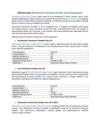
At SQPCB, our production line for printed circuit boards includes everything from raw material cutting to final inspection. With capabilities up to 24 layers, heavy copper, rigid-flex, and large board sizes, we ensure your production boards meet demanding technical specifications.

E N D
Imagine squeezing the power of a supercomputer into your smartphone. That's the magic of SQPCB technology. It packs more circuits into tiny spaces without losing speed or strength. As devices get smaller, SQPCB steps up to handle the heat. SQPCB stands for Stacked Quality Printed Circuit Board. This advanced type builds on basic PCBs but stacks layers with top-notch precision. It solves big problems in today's gadgets like 5G phones and smart home sensors. Demand for SQPCB production grows fast. The global PCB market hits $70 billion in 2023, with high-density boards taking a bigger slice each year. Defining SQPCB and Its Market Relevance Traditional PCBs use simple FR4 material for everyday boards. SQPCB goes further with stacked layers that connect in smart ways. It tackles tight spaces and heat buildup that plague older designs. Engineers turn to SQPCB for reliable performance in crowded electronics. Think of AI chips or wearables where every millimeter counts. This tech cuts signal loss and boosts speed in fast networks. The Performance Edge: Why Engineers Choose SQPCB SQPCB shines in key areas like impedance control. That means signals travel without distortion over long traces. You get clean data in high-speed apps. Signal integrity stays strong even in dense setups. Miniaturization lets you fit more features without bulking up the board. No wonder teams pick it for cutting-edge hardware. Engineers love how SQPCB handles tough jobs. It supports faster data rates, up to 100 Gbps in some cases. Reliability jumps, cutting failures by 30% over standard boards. Section 1: Core Technologies Enabling SQPCB Fabrication Building SQPCB demands smart tech at every step. These methods create dense, sturdy boards that last. Let's break down the basics. Advanced Lamination and Interlayer Bonding
Lamination glues layers together under heat and pressure. Special glues prevent air pockets that weaken bonds. High temps, around 200°C, ensure tight fits in fine-pitch boards. You need tough dielectric materials here. They resist cracks during stacking. This keeps multi-layer boards flat and strong for assembly. Without solid bonding, delamination hits hard. Factories use vacuum presses to suck out air. That boosts yield by 15% in production runs. Microvia and HDI Integration Techniques High-Density Interconnect, or HDI, packs vias close together. Laser drilling with excimer tools carves tiny holes, just 50 microns wide. Depth control stays precise to avoid shorts. Stacked vias link layers in clever stacks. Staggered ones save space, while back-drilled clear extras for clean signals. Aspect ratios hit 1:1 for deep connections. These techniques make SQPCB flexible. You route signals through multiple levels without waste. It's key for compact designs in IoT gear. Material Selection: Low-Loss Dielectrics Pick substrates like PTFE for high frequencies. They have low Dk values, around 2.5, to slow signals less. Df stays under 0.002 for minimal loss. Advanced polyimides handle heat up to 250°C. They suit AI hardware with power draws. Match materials to your project's needs. Wrong picks cause signal fade. Test samples early to lock in the best fit. This step saves headaches later. Section 2: Precision Imaging and Etching Processes Fine lines define SQPCB success. Imaging and etching carve paths with micron accuracy. Get this right, and your board hums. Direct Imaging (LDI) vs. Traditional Phototooling LDI uses lasers to draw patterns straight on the board. It skips film, cutting errors by 50%. Throughput speeds up for big batches. Old phototools rely on masks that wear out. LDI adjusts on the fly for tweaks. Ideal for SQPCB's ultra-fine needs. Switch to LDI, and waste drops. Panels align better, raising output. Controlled Impedance Trace Etching
Wet chemicals etch traces to exact widths, like 25 microns. This keeps impedance steady at 50 ohms for digital lines. Uniformity spreads even across 18x24 inch panels. Control etch rates with fresh baths. Additives stop undercuts that ruin shapes. Vital for high- speed ports like USB4. Test traces post-etch. Tools measure resistance to confirm specs. Small tweaks prevent big issues down the line. •Use ferric chloride for clean etches. •Monitor pH to avoid rough edges. •Rinse well to clear residues. Surface Finish Selection for Advanced Assembly ENIG coats pads with gold over nickel. It fights oxidation in fine-pitch parts. ENEPIG adds palladium for better wire bonds. Organic preservatives protect without metal layers. Pick based on your solder type, like lead- free. These finishes aid tiny BGA chips on SQPCBs. Match finish to assembly heat. Gold lasts but costs more. Balance needs with budget for smooth runs. Section 3: Sequential Build-Up and Reliability Testing SQPCB builds layer by layer, like stacking bricks. Each step checks for flaws. Testing seals the deal on quality. The Sequential Build-Up Manufacturing Strategy Start with a core substrate. Image and etch it first. Drill microvias next, then plate to fill. Laminate more layers on top. Repeat imaging and plating. Outer layers get final touches before routing. Control temps at each phase. Variations cause warps. This method ensures even stacks up to 20 layers. Plating Technology for High Aspect Ratio Vias Pulse plating sends bursts of current. It fills deep vias without gaps. Special baths with copper sulfate work best. Aspect ratios reach 10:1 for stacked setups. Electrolytes add brighteners for smooth walls. Voids drop to under 1%. Monitor thickness with coupons. Adjust voltage for full coverage. Key to avoiding open circuits.
Non-Destructive Quality Assurance (QA) Protocols X-rays spot voids in vias fast. No cuts needed. AOI scans traces for breaks or extras. Run Thermal Cycling Tests at -40°C to 125°C. Stacked boards endure 1000 cycles without cracks. Flying probe tests check continuity. Layer these checks in. Early catches save rework costs. Aim for 99% pass rates. •X-ray: Detects hidden flaws. •AOI: Flags surface defects. •TCT: Proves long-term strength. Section 4: Challenges and Optimization in SQPCB Production Scaling Scaling SQPCB from lab to factory tests skills. Hurdles pop up, but fixes exist. Optimize to keep costs down. Yield Management in High-Density Fabrication Dust in lamination kills yields. Clean rooms with HEPA filters help. Bad plating leaves voids that fail tests. Use SPC to track stats. Plot via fill rates daily. Adjust processes when trends dip. Tips include: •Train staff on clean handling. •Calibrate lasers weekly. •Batch small at first to learn. Yields climb from 70% to 95% with tight control. Thermal Management Challenges in Small Form Factors Dense boards trap heat from chips. Add thermal vias in arrays to vent it. Copper pours spread warmth evenly. Pick cores with high thermal conductivity, like 2 W/mK. Embed heat sinks during build. This cools hotspots in tight spots. Design with sim software first. Test prototypes under load. Avoid melts in power-hungry apps. Cost Drivers in Advanced PCB Manufacturing
Special materials like PTFE jack up bills by 3x over FR4. Lasers and imagers depreciate fast, adding $0.50 per square inch. Inspections take time, doubling labor. Compare to standard boards: SQPCB costs 2-5 times more. Volume drops per-unit price. Cut costs with panel sharing. Reuse setups for repeats. Balance quality against spend. Conclusion: The Future Trajectory of SQPCB Integration SQPCB production blends art and science for tiny powerhouses. It demands precision in stacking, etching, and testing. Mastering this gives your projects an edge in speed and size. Look ahead to new materials like flexible hybrids. They promise even smaller boards for foldables. Trends push toward 3D printing vias, slashing times. Key Takeaways for Design and Procurement Teams •Watch tolerance stacks in layers to avoid misfits. •Spec low-loss materials for signal paths. •Plan thermal paths early in layouts. •Test for 1000+ cycles in harsh spots. •Partner with fabs that hit 95% yields. Ready to build your next SQPCB? Reach out to experts and start prototyping today. Your innovations await.