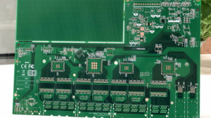
In the selection of PCB surface finishing processes, OSP (Organic Solderability Preservative) holds a prominent position due to its unique advantages. However, engineers often find that OSP is far from the best solution when assembling complex boards that require double-sided mounting or multiple soldering passes. Why does this process fall short when faced with "secondary reflow"?
1. What is OSP?
OSP is a chemical process that forms an extremely thin, organic film on the surface of the PCB's copper foil. This film typically measures only 0.2 to 0.5 micrometers in thickness. Its core function is straightforward: to protect the copper surface from oxidation before soldering occurs. Crucially, during the soldering phase, the film must be quickly dissolved by the flux, exposing the fresh copper so it can bond with the solder.
2. Core Advantages and Limitations of OSP
OSP's popularity stems primarily from its significant advantage in low cost, as it doesn't require expensive plating equipment. Furthermore, because the film is so thin, it offers exceptional pad flatness, which is vital for the successful soldering of fine-pitch components and BGA packages. Additionally, it is inherently lead-free and environmentally friendly.
However, OSP's drawbacks are equally pronounced: the protective film is very fragile, easily susceptible to scratches, and requires extremely strict storage conditions (including vacuum packaging and humidity monitoring) due to its limited shelf life.
3. Why OSP Is Unsuitable for Secondary Reflow Soldering
For PCBs requiring double-sided component mounting (meaning they must pass through the reflow oven twice), OSP is usually not the preferred choice. The main reasons lie in the "single-use" nature of its protective film and its insufficient heat resistance.
- Thermal Decomposition and Film Failure: OSP's operating principle dictates that it must decompose easily at high temperatures. During the first reflow cycle (soldering the first side), the entire PCB is subjected to high heat. The OSP film on the second, un-soldered side (or on through-holes) is simultaneously hit by this thermal shock. Studies indicate that the protective film can be completely broken down or chemically altered during this initial high-temperature exposure. Once the film is compromised in the first pass, the exposed copper is left unprotected in the presence of hot air.
- Accelerated Oxidation Leads to Poor Solderability: High temperature is a catalyst for oxidation. After the OSP film fails in the first reflow, the oxidation rate of the copper pads on the second side accelerates significantly. When the PCB enters the second reflow cycle, the OSP layer that should have protected the copper is no longer functional. What remains is a layer of copper oxide formed under high heat. This stubborn oxidation layer is extremely difficult for the flux to remove effectively, ultimately leading to poor wetting, weak solder joints, or even component rejection on the second side.
- Inability to Protect Non-Pad Areas: Furthermore, OSP only protects the surface pads, not the inner walls of through-holes (if the through-holes require subsequent soldering or testing). Under multiple thermal shocks, the copper inside these holes can oxidize, compromising future testing or electrical reliability.
Conclusion
In summary, while OSP excels in flatness and cost efficiency, its inherent poor resistance to multiple thermal exposures makes it a significant risk in the secondary reflow process. For complex boards requiring high reliability or multiple reflow cycles, selecting a more durable, heat-resistant surface finish like ENIG (Electroless Nickel Immersion Gold) is consistently the smarter and safer engineering choice.