Download
1 / 8
80 likes | 115 Vues
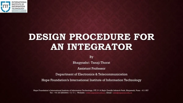
This presentation provides information on Design Procedure for Integrator and is presented by Prof. Bhagyashri Tanaji Thorat, from the department of Electronics & Telecommunication at International Institute of Information Technology, I2IT. The presentation shows circuit diagram of an integrator and solution equations.

E N D
Design procedure for an Integrator By Bhagyashri Tanaji Thorat Assistant Professor Department of Electronics & Telecommunication Hope Foundation’s International Institute of Information Technology Hope Foundation’s International Institute of Information Technology, I²IT, P-14 Rajiv Gandhi Infotech Park, Hinjawadi, Pune - 411 057 Tel - +91 20 22933441 / 2 / 3 | Website - www.isquareit.edu.in ; Email - info@isquareit.edu.in
Design procedure for an Integrator • If gain is not given in problem statement assume gain =10 • From the value of gain. Assume R1& calculate RF. • Calculate fa from fb • Calculate from the value of • Calculate Hope Foundation’s International Institute of Information Technology, I²IT, P-14 Rajiv Gandhi Infotech Park, Hinjawadi, Pune - 411 057 Tel - +91 20 22933441 / 2 / 3 | Website - www.isquareit.edu.in ; Email - info@isquareit.edu.in
Problem statement to design Integrator Design a practical Integrator circuit to properly process input sinusodial waveform upto 1kHz . The input amplitude is 10 mV. Hope Foundation’s International Institute of Information Technology, I²IT, P-14 Rajiv Gandhi Infotech Park, Hinjawadi, Pune - 411 057 Tel - +91 20 22933441 / 2 / 3 | Website - www.isquareit.edu.in ; Email - info@isquareit.edu.in
Circuit diagram Integrator Hope Foundation’s International Institute of Information Technology, I²IT, P-14 Rajiv Gandhi Infotech Park, Hinjawadi, Pune - 411 057 Tel - +91 20 22933441 / 2 / 3 | Website - www.isquareit.edu.in ; Email - info@isquareit.edu.in
Solution • Given • Assume dc gain 10 Hope Foundation’s International Institute of Information Technology, I²IT, P-14 Rajiv Gandhi Infotech Park, Hinjawadi, Pune - 411 057 Tel - +91 20 22933441 / 2 / 3 | Website - www.isquareit.edu.in ; Email - info@isquareit.edu.in
solution • Substituting value of Hope Foundation’s International Institute of Information Technology, I²IT, P-14 Rajiv Gandhi Infotech Park, Hinjawadi, Pune - 411 057 Tel - +91 20 22933441 / 2 / 3 | Website - www.isquareit.edu.in ; Email - info@isquareit.edu.in
solution Calculate = ≈ Hope Foundation’s International Institute of Information Technology, I²IT, P-14 Rajiv Gandhi Infotech Park, Hinjawadi, Pune - 411 057 Tel - +91 20 22933441 / 2 / 3 | Website - www.isquareit.edu.in ; Email - info@isquareit.edu.in
Thank You For further details please feel free to contact BhagyashriThorat Department of Electronics & Telecommunication Hope Foundation’s International Institute of Information Technology, I²IT P-14, Rajiv Gandhi Infotech Park, MIDC Phase 1, Hinjawadi, Pune – 411 057 Tel +91 20 22933441 / 2 /3 www.isquareit.edu.in bhagyashrit@isquareit.edu.in | info@isquareit.edu.in