Download
1 / 1
10 likes | 250 Vues
250 nm. 1.1. 1.3. 1.15. 1.2. 1.25. 1.2. Assembled NEMS. Buried Electrode. Top Electrode. Au. SnO 2. Au. Assembled NEMS. Buried Electrode. Top Electrode. Integration of Nanosensors. MUX. Nanowire. R. 1. (R. ). X. +. R. R. V. 2. 3. OUT. Readout. _. CMOS Two - Stage.

E N D
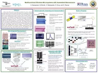
250 nm 1.1 1.3 1.15 1.2 1.25 1.2 Assembled NEMS Buried Electrode Top Electrode Au SnO2 Au Assembled NEMS Buried Electrode Top Electrode Integration of Nanosensors MUX Nanowire R 1 (R ) X + R R V 2 3 OUT Readout _ CMOS Two - Stage Differential Amplifier Multifunctional Wireless Microsystems with Assembled Nanosensors A. Narayanan, N.DiLello, V. Deshpande, S. Evoy, and S. Raman Abstract Dielectrophoretic Assembly and Characterization Work in Progress Wireless Sensor Microsystems are expected to revolutionize the security, control and monitoring operations of commercial, military and industrial systems. We present a technique that enables integration of nano-scale sensor devices with low-power CMOS Integrated Circuits, in particular, sensor readout, data conversion and wireless communication functionalities. At present, we have demonstrated the assembly of nanowires such as metallic nanowires and carbon nanotubes onto lithographically defined electrodes fabricated on a Si chip for proof of concept purposes. The nanowires are assembled between two electrodes by applying an alternating electric field across the electrodes. The placement and alignment of the nanowires are defined by dielectrophoretic forces that act on the nanowires. Characterization of the assembled wires and carbon nanostructures is also presented. We plan to extend this work to provide a new dimension in multifunctional sensor systems. The technique described above allows for the sequential assembly of diverse functionalized nanosensor elements onto a single-chip system. For example, the sensing nanostructures can be straightforwardly integrated with a low-power frequency-hopped spread spectrum transmitter. The proposed transmitter architecture allows a large number of sensor nodes to communicate within each other and also with the central control unit at low-to moderate data rates. With integration of diverse functionalized nano-scale sensors with low-power read-out and data communication system, a versatile and commercially viable low-power wireless sensor system can be realized. • Synthesis, Characterization and Integration of segmented chemresistive nanowires • Alternating Electric field is provided to the buried electrodes • Top electrodes laterally confine the field lines • Dielectrophoretic forces manipulate the nanowires • Charge separation induces assembly along field lines • Length of Nanowire = 2.5 um Diameter = 260 nm • Mechanical resonance observed at 23 MHz Why Integrated Nanosystems? 200 nm • Integration of diverse functionalized nano-scale sensors with low- power readout, signal conditioning and data communication circuits • Single-chip wireless sensor microsystem Wireless sensor networks Assembled Rh NEMS Micro-scale Nano-scale • Low power consumption • Smaller Dimensions Large number of sensor arrays in one system • Convenient detection of ultra-small forces and masses • Added versatility to silicon ICs • Assembled multiwalled- nanotubes on Si circuits • Mechanical resonance observed at 1.2 MHz ; Q = 130 Architecture of Wireless Sensor Networks Multiwalled-nanotubes D. W. Carr, S. Evoy, L. Sekaric, J. M Parpia and H. G. Craighead, Appl. Phys. Lett. (1999). Sandia Natl. Labs. And How? Event • Diameter = 250nm Thickness of walls = 15nm • Semiconducting behavior observed • The “Bottom-Up” Approach – structure sizes from nano-scale down to molecular scale can be realized • Better features than “Top-down” approach • Better resolution • Provides intrinsic structural handles for the development of functional sensing responses into the device Carbon pipes A/D Converter Nanowire Assembly Sites Diverse functionalized nanosensors Integration with CMOS Operating Circuitry Development & Integration of Nanostructures Frequency-hopped Spread Spectrum Transmitter • Circuit Design and Layout performed using Motorola HiP6WRF low-voltage 0.18 um Si/SiGe BiCMOS process (CMOS platform technology) • Assembly electrodes in Metal 5 and buried electrodes in Metal 4 • Passivation layer opened up to enable assembly of nanowires • Integrated Readout circuit Resistance measuring circuit with CMOS differential amplifier for proof of concept • Currently being refabricated – fabrication problems encountered due to layout error Provides multi-user environment Low-power operation Free from Interference Au/Ni/Rh nanomagnetic cantilevers – Magnetically active devices consisting of Ni particle grown onto stiff Rh support Chemresistive Au/SnO2/Au volatile compound sensing nanostructure Magnetic Clusters in nanotube Acknowledgements Penn State UPenn Motorola Layout of assembly sites and cross-sectional view of CMOS process • Saramma Varghese, UG • Tushar Jaruhar, MS • Papot Jaroenapibal, Ph. D • Prof. David Luzzi • Prof. Y. Gogotsi • Ben Martin • Irena Kratochvilova • Prof. Thomas Mallouk • Prof. Theresa Mayer • Michael Clifford • Chris Magnella • Eric Maass Nanostructures are developed using“bottom-up”approach Nanostructures are integrated onto a chip using Dielectrophoretic assembly technique Schematic of readout circuit