Lecture 3
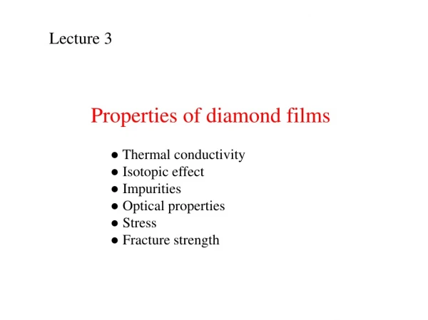
Lecture 3. Properties of diamond films. ● Thermal conductivity ● Isotopic effect ● Impurities ● Optical properties ● Stress ● Fracture strength. Thermal conductivity of diamond and some optical and electronic materials at room temperature. bulk materials.

Lecture 3
E N D
Presentation Transcript
Lecture 3 Properties of diamond films ● Thermal conductivity ● Isotopic effect ● Impurities ● Optical properties ● Stress ● Fracture strength
Thermal conductivity of diamond and some optical and electronic materials at room temperature bulk materials 3 GHz, 50 W transistor on CVD diamond heat spreader. “Pulsar” company, Moscow ● thermal conductivity of diamond: 5 times higher than for copper, and 50 times higher than for sapphire. ● ultimate bulk material for thermal management and high power optics.
Anisotropy of thermal conductivity in polycrystalline CVDdiamond Phonon scattering on grain boundaries. Columnar grain structure TC anisotropy. Depth inhomogeneity due to crystal size variation. Perpendicular values k should higher than the in-plane values k. J. Graebner, et al., J. Appl. Phys. 71 (1992) 5353.
IR detector laser beam sample metal film (absorber) Measurements of thermal diffusivity by Laser Flash Technique (LFT) ●Delivery of laser pulse through an optical fiber to improve uniformity of irradiation on the sample. ● Software for automatic evaluation of thermal diffusivity and TC. ●Vacuum Cryostat. Measurements thermal diffusivity in the temperature range 180 – 430 К. ● LFT measures perpendicularthermal diffusivityD. Method: heating of the front side by short laser pulse and tracing the T(t) on rear side. Temperature evolution (T(t) on rear side of the film
He - Ne Nd:YAG Transient thermal grating technique measures parallelthermaldiffusivityD • ●thermal grating formation due to • refraction coefficient modulation by • two interfering laser (Nd:YAG) beams. • ● diffraction of probe He-Ne laser beam • on the transient grating with period Λ. Diffraction signal decay due to thermal dissipation
Set-up for DIImeasurement using thermal grating technique Period of thermal grating 30-120 µm E.V. Ivakin, QuantumElectronics(Moscow),32 (2002) 367.
Thermal conductivity at room temperature sensitive to content of hydrogen impurity in diamond ● Bonded hydrogen (C-H) decorates defects and grain boundaries. ● Hydrogen concentration as an indicator the defect abundance in CVD diamond. K┴ K║ ● Thermal conductivity as high as 2100 W/mK. ● anisotropy: k (perpendicular ) > k (in-plane); Δk/k=10-15%. A.V. Sukhadolau et al. Diamond Relat. Mater. 14 (2005) 589
Thermal conductivity k┴ vs hydrogen impurity in diamond Open squares – samples from Element Six [S.E. Coe, Diamond Relat. Mater. 9 (2000) 1726]; full squares – GPI samples. V. Ralchenko, in Hydrogen Materials Science and Chemistry of Metal Hydrides, Kluwer, 2002, p. 203.
Thermal conductivity along diamond wafer as measured by LFT at room temperature disk diameter 63 mm, thickness 1.28 mm k, W/cmK Distance along disk diameter, mm
Correlation of optical absorption and parallel thermal conductivity Absorption spectra in the visible In agreement with the correlation found by J. Graebner, DRM,4 (1995) 1196 for white light absorption and k. At least a part of defects contribute both in enhanced absorption and in thermal resistance. A.V. Sukhadolau et al. Diamond Relat. Mater. 14 (2005) 589
Thermal conductivity kII at elevated temperatures The decrease of thermal conductivity with T is mostly due to phonon-phonon scattering mechanism (phonon population increases with T). Well fitted with the relationship k ~ T –n (solid lines). • Samples compared: • - undoped diamond film (poly), • B-doped film poly); • type IIa single crystal diamond • [T.D. Ositinskaya, Superhard Materials (Kiev), No. 4 (1980) 13].
k(T) : general form for an insulator Heat is transferred by phonons k = ⅓ C(T)· v· λ(T) C is the heat capacity per unit volume, v is the average phonon velocity, λ is the mean free path of phonons between collisions. Any phonon scattering mechanism reducing λ decreases the thermal conductivity. scattering on boundary phonon-phononscattering defects ● The peak in k occurs at a temperature about 10% of Debye temperature, D. ● At low T: λ is constant, and k ~C(T) ~ T3. ● Phonon-phonon scattering dominates at high T (k~ T-1). ● Scattering on defects is essential at intermediate temperatures.
Temperature dependence of thermal conductivity for certain crystals k, W/mK Occurrence a maximum in k(T) at low temperatures (80-100 K). Diamond – not the champion in the value of maximum TC, but its k is uniquely high at high temperatures (T>70K), particularly at room temperature. This is the consequence of record high Debye temperature θD =1860K for diamond (very high phonon frequencies are excited). R. Berman, Diamond. Res. (1976)
Thermal conductivity kII at elevated temperatures T = 293-460 K Exponent n = 0.17 – 1.02 increases with diamond quality Approximationk ~ T –n • ● Comparison with data for single crystal natural diamonds [ Burgemeister, Physica, 1978]. • ● Weak temperature dependence for highly defective CVD diamond. ● Concentration of H impurity (in ppm) is indicated for each sample. ● The data for isotopically pure (12C) synthetic HPHT single crystal diamond [Olson PB’1993] give n=1.36, the highest slope for any diamond. A.V. Sukhadolau et al. Diamond Relat. Mater. 14 (2005) 589
Defects in transparent CVD diamond (poly) GB - grain boundaries T - twins SF - stacking faults D - dislocations L. Nistor et al, Phys. Stat. Sol.(a), 174 (1999) 5.
Typical dimensions of defects Point defects are atomic scale defects: - isolated foreign atoms; - different isotopes; - vacancies Nitrogen ~ 1 ppm or less Boron << 1ppm Hydrogen 20 -1000 ppm (poly) Vacancies - few ppm (?) Isotope 13C ~10,000 ppm (main impurity!) Scattering rate of phonons with frequency ωon isotopic atom with mass m +Δm: 1/τiso = Ãisoω4 Ãiso = Ciso(V0/4πv3)[Δm/m]2 Ciso is isotope concentration, V0 is atomic volume, v is sound velocity. For diamond Δm=1 : Aiso(nat) = 4.045 × 10⁻³ c-1K-1. Defects present in polycrystalline CVD diamond and their scale K.J. Gray, Diamond Relat. Mater. (1999)
Thermal conductivity of isotopically “pure” diamond Is it possible to increase K for diamond above 2400 W/mK at room temperature? Natural and synthetic diamonds (and any carbon material) contain 1.1% of isotope 13C.The 13C atoms are scattering centers for phonons – carriers of heat, thus restricting the thermal conductivity of diamond. Concentration of 13C isotope is much higher than other impurities–point defects. Solution – eliminate 13C isotope from CVD diamond.
Isotopic effect on thermal conductivity of diamond The ultimate opportunity to achieve TC values > 2400 W/mK relays on purification of isotopic composition of diamond. The natural isotope content in diamond is 98.93% 12C and 1.07% 13C. Phonon scattering on 13C atoms results in thermal resistance. Previous works Si diamond Isotopically modified 12C (99.90%) single crystalHPHT diamond, General Electric (1990-1993) k=33.2 W/cmK 50% increase vs “normal” diamond. L. Wei, PRL, 70 (1993) 3764 12C-enriched polycrystallineCVD diamond films: k = 21,8 W/cmK; k = 26 W/cmK G.E. Graebner, Appl. Phys. Lett. 64 (1994)2549. Highly enriched (99.98%) 28Si. At room temperature: thermal conductivity enhancement of 10% compared to k = 140 W/mK for natural Si. In the maximum at 26K the TC gain is 8 times. R.K. Kremer et al. Sol. State Comm. 131 (2004) 499.
Growth of isotopically enriched poly12C CVD diamond ● production of 12CO with purity 12C 99.96% ● conversion to 12CH4 ● diamond deposition by MPCVD (purity is preserved) ● cutting to 12x2x0.46 mm3 bar ● TC measurements, steady state method CO isotope separation by diffusion. “Colonna” system, Kourchatov Institute, Moscow. k = 2510W/mK at 298K for 12C diamond (higher than for type IIa single crystals) - isotopic effect of 32%. k = 1900W/mKfor 0.5 mm thick film with natural isotope abundance. k=2600W/mK- perpendicularly to the film plane. The isotopic effect increases with temperature decrease - the maximum TC of 4700 W/mK at T=160K. A. Inyushkin et al. Bull. Lebedev Phys. Inst. 34 (2007) 329 The further increase in TC for 12C diamond is limited by defects, impurities, grain boundaries. ► single crystals
Measurement cell to determine thermal conductivity at T = 4 - 450K Steady state method of constant thermal gradient. Sample – polycrystalline CVD diamond. The cryostat in vacuum lower 10-5 Torr. Multilayer thermal radiation shield (at T>200K). Measurement accuracy of k is better 3% (primarily due to an error in distance between thermometers). Copper block Diamond bar 14x2x0.5 mm3 Resistor thermometer (Cernox, LakeShore Cryotronics) Heater (resistor) Kourchatov Institute, Moscow
Applications of isotopically modified diamonds with extraordinary thermal conductivity ● Heat spreaders for high power electronic devices ● Single crystals and nanocrystals with nitrogen-vacancy (NV) fluorescent color centers for quantum computing and cryptography - isotope 13C with nuclear spin should be eliminated to increase spin relaxation (coherence) time of NV centers to µs level. ● Reflecting and transmission X-ray optics for high intensitybeams (synchrotron sources) a combination of high TC, low atomic number Z and structure perfection is required. ● Laser optics (including diamond Raman lasers) with increased damage threshold.
Thermalconductivity of UNCD measured by a laser flash technique ● k = 0.06-0.10 W/cmK at RT is 200 times lower than for single crystal diamond, but still higher than for amorphous sp3 carbon ta-C ka-C= 0.035 W/cmK. ● Thermal conductivity decreases with nitrogen “doping”. ● k = 1/3 C*V*L, where C – heat capacity, V – sound velocity, L – phonon free path. For single crystal L=240 nm; for NCD L2 nm (of the order of grain size). Thermal conductivityvs N2% V. Ralchenko, et al. DRM, 16 (2007) 2067
Thermalconductivity of UNCD Temperature dependences measured by “3 Omega” method W.L. Liu et al.APL 89 (2006) 171915 a-C ● kNCDis between polycrystalline diamond and amorphous carbon; ● slow and monotonic temperature dependence; ● in a phonon-hopping model (PHM) the reduction in thermal conductivity is due to decrease in phonon transparency parameter (t) through grain boundaries: t=0.2-0.32 for UNCD, t=0.9 for polycrystalline film.
Nitrogen and hydrogen impurities in CVD diamond N and H content evaluation from optical absorption spectra N-induced UV absorption 270 nm C-H stretch absorption bands 2800-3100 cm-1 2-phonon absorption Diamond samples of different qualities A - E S. Nistor et al. J. Appl. Phys. 87 (2000) 8741.
Correlation of (bonded) H and N impuritiesHydrogen and nitrogen concentrations are determined from IR and UV absorption V. Ralchenkoet al. in Hydrogen Materials Science and Chemistry of Metal Hydrides, Kluwer, 2002, p. 203; A.V. Sukhadolau et al. Diamond Relat. Mater. 14 (2005) 589.
Luminescent nitrogen-vacancy (N-V) and nitrogen-vacancy (Si-V) color centers in diamond PL spectrum on moderate quality of polycrystalline diamond film. ● Bright PL lines на 637 nm (1,945 эВ) from NV-and 575 nm from NV0. ● PL lines на 738nmfrom SiV. ● All these centers are stable at room temperature. ● Dopingduring growth process
Si impurity in CVD diamond: depth mapping V. Ralchenko, inNanostructured Thin Films and NanodispersionStrengthened Coatings, 2004, p. 209. Mapping PL in cross section The diamond films were deposited on Si substrate at temperature 700ºC (squares) and 800ºC (triangles), and on Mo substrate at 700ºC (circles). Si impurity extends to 20-60 μm in depth. Si-diamond interface
Optical transmission Extremely broad transparency window: from UV to RF, including THz range ● Cut-off wavelength 225 nm. ● 2-phonon absorption band at 2.5- 6.3 µm ● Loss tangent 10-5 at 170 GHz.
Optical transmission in UV and visible range for natural IIa type single crystal diamond and poly CVD film absorption and scattering on defects and grain boundaries
Polycrystalline CVD diamond as material for high power CO2laser windows Non-contact phase photothermalmethod to absolute measurements of optical absorption coefficient The absorption of heating CO2laser (λ=10.6 μm) leads to local variable (at the modulation frequency) heating and to changes in the refractive index, which, in turn, caused the change in the phase difference between two probe beams of He-Ne laser (633 nm) detected by the probe interferometer. Simulation and experiment show that the level of low absorption achieved is enough for use of CVD diamond as window of multi-kilowatt cw CO2 lasers. A.Yu. Luk’yanov, QuantumElectronics (Moscow) 38 (2008)1171
Dielectric losses in CVD diamond (170 GHz) ● Far infrared (Microwave) absorption of dielectrics is due to lattice absorption owing to unharmonism (two phonon absorption - TPA). Diamond has very low TPA, hence low loss tangent. ● Theory: tgδ ~109 for λ=2 mm (150 GHz) [B. Garin, JTP Lett. 1994, No. 21, p.56]– record low for any material. Compare with tgδ ~105 for Si. ● Experiment: best result tgδ ~ 3106@ 140 GHz for Element Six polydiamond. Sample: GPI 0.74 mm thick diamond film tgδ ~105 stable up to 400ºC B. Garin et al. Techn. Phys. Lett. 25 (1999) 288
MicroRaman mapping of stress in diamond films The confocal optical scheme – high spatial resolution ◄ no stress ◄ compressive stress ◄ tensile stress Raman spectra taken at 5 different locations on the surface of diamond film within one grain (≈100x100 µm). The shift of the peak from 1332. 5 cm-1 position is the evidence of stress.
MicroRaman stress mapping on a surface over a selected 160x160 μm grain in the diamond film local stress regions [cm-1] = -2.2 [GPa] stress along (111); [cm-1] = -0,7 [GPa] stress along (100). max ≈ 6 cm-1max ≈ 3 GPa I.I. Vlasov, Appl. Phys. Lett. 71 (1997) 1789.
MicroRaman Stress mapping around grain boundary laser beam scanning in depth and along the surface in-depth, grain B in-depth, grain A lateral, from A to B I. Vlasov, Physica Status Solidi (a), 174 (1999) 11.
Fracture strength by 3-point measurement techniques Advantage of 3 point method: ability to handle with small size samples Observation: the fracture happens close to the central part of the bars (in locations of maximum stress) Testing apparatus at Fraunhofer Institute IAF, Friburg (1) Fracture strength Young’smodulus (2) b and h are the specimen width and thickness, Fс is critical load value, l= 7.8 mm is distance between supports, Dis displacement of the bar under load (measured by an inductive sensor with a resolution ~ 1µm). Similar principle atUSTB (Beijing) DF-100 test unit bar thickness of 0.5 mm only L = 8 mm, loading rate 0.5 N/s two supporting cylinders 3mm diameter. V.G. Ralchenko et al.Diamond and Related Materials 23 (2012) 172.
Fracture strength vs film thickness white diamond Grain size ranges with thickness from 10 µm to ~ 200 µm σfr = 400 - 1400 MPa for 0.5 mm thick plate ● Rapid increase in strength towards small thickness h: σ= 600 MPa @ h ≈ 1000 µm ► 2.2 GPa @ h = 60 µm (nucleation side in tension). ● Similar tendency for growth side. ● Compatible with Hall-Petch relation if the length of critical cracks is proportional to grain size. ● Results similar to Element Six data. ● The Young’ modulus of Е=1072 ± 153 GPameasured from the bending tests is only 10% lower compared to therotetical Young’ modulus of polycrystalline diamond.
Fracture strength vs grain size Hall-Petch relationσf = σ0 +Kd-1/2 Growth side and substrate side are under tensile load.White diamond.
Fracture patterns close to growth and nucleation sides white diamond Growth side, top view – evidence of transgrain fracture Growth side Cleavage steps Nucleation side ●Transcrystallitefracture over entire film thickness ● Strong grain boundaries
Fractures statistics. Weibull analysis for white diamond P(σ) = 1 – exp[– (σ)/σN)m] m is Weibull modulus, can found from slope of eq. or ln[–ln(1 – P)] = – mln(σN) + mln(σ) High m value means more narrow strength interval (more predictable behavior). Nominal strength σN = 550 MPa for growth side in tension σN =1060 MPa for substrate side in tension Higher modulus m for growth side
Comparison of fracture strength of white and black diamond film thickness 0.5 mm Independent on what side is under tension, a factor of 2 – 2.5 lower σ for opaque material in spite of the smaller grain size.
Black diamond. Fracture surface Cleavage along GB ►smooth surface planes along boundaries of columnar grains ► reduced bending strength intergranular fracture transgranular fracture Growth side Nucleation side Area in the middle of the cross- section Columnar structure is seen even in a few microns thin layer adjacent to the substrate.