Download
1 / 23
230 likes | 483 Vues
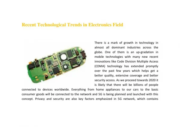
Circuit boards are extensively used across in the electronics industry. So much so that nowadays a circuit board designer is expected to be also proficient in the manufacturing technology apart from understanding electrical engineering. Read this article which will provide you with an insight on the various current and emerging technological trends prevailing in the manufacture of printed circuit boards.

E N D
Technological Trends in the Field of Circuit Board Design & Manufacturing Published by:
Introduction Circuit boards are found in all electronic products.The advancement in semiconductor technology is driving the giant electronics industry. PCB industry has been quickly responding to the rapidly evolving global electronics market. Today, circuit board designers should have a thorough knowledge of both electrical engineering and manufacturing technology. Collaborating with EMS vendors during early stages will helps the designers to reduce design risks and find cost effective solutions. This article will provide a brief overview of the technological trends prevailing in the field of printed circuit technology and serve as a walkthrough to the lesser known technologies in the printed circuit market. CHAIRMAN
Market trends: CHAIRMAN
Asian countries continue to fulfil the majority of the global PCB demand. China, South Korea, and Taiwan continue to fulfill the huge demand created by markets for smartphone, tablet computers, display monitors, and TV. Export to western countries also accounts for a major chunk of the global PCB demand because of highly competitive pricing offered by the Asian PCB manufacturing industry. The European PCB industry focuses on low volume and high-end markets like instrumentation and control, automotive, medical, military, and aerospace. Production in North America is dominated by the USA, largely occupied by military, aerospace and defense sectors. From technological point of view, a standard multilayer PCB still commands a large share of the market. With global trend of miniaturization of electronic products, HDI and Rigid-Flex technology will continue to grow in future. CHAIRMAN
Industry Challenges With advancement in ICs package technology, mobile revolution, and IOT kicking in, PCB geometries will continue to shrink. Designing ultra-thin printed circuit boards which meets the required signal integrity and EMC specifications at low cost will be challenging. CHAIRMAN • Technology Trends • Printed circuit boards can be broadly classified into: • Conventional PCB (Single-sided, Double-sided and Multilayer PCB) • Flexible and Rigid-Flex PCB • High Density Interconnect (HDI)
CHAIRMAN Example HDI board using “2-N-2” HDI Buildup (N = number of standard layers)
HDI technology has been used in manufacturing products like wearables, smartphones, and tablet devices. One of the major challenges faced by the PCB industry is increasing the layer count and reducing the thickness of the circuit boards without compromising the structural rigidity and electrical performance of a PCB. The average thickness of a PCB is around 0.5 mm to 0.7 mm and is expected to be less than 0.4 mm in next few years. Compared to the 0.7mm pitch BGA package used in smartphones a few years ago, latest smartphones uses 0.4 mm pitch BGA package which offers a higher pin count in smaller PCB real estate. The IC industry has already been working on 0.3mm pitch BGA technology for next generation microprocessors and FPGAs. CHAIRMAN
IC substrate manufacturers have developed “mSAP” (Modified Semi Additive Process) process which is capable of creating fine lines with better conductor geometry. The HDI PCB industry is adapting to the mSAP process to tackle the upcoming challenges. While 90% of production uses the Contact Imaging Process today. Laser direct imaging (LDI) looks like a promising technology for the future. With 0.3 mm pitch BGA, microvia pad/hole size is expected to be in the order of 150um/75um, respectively. While, PCB industry will continue to use CO2 laser for drilling microvia in near future. New lasers with picosecond pulse are coming to the market which offers finer holes and drastically lower thermal damage. ALV (Any Layer Via) HDI technology is currently expensive and requires a state-of-the-art facility. In coming years, 10 to 12 layer microvia layer buildup will be common in next generation handheld and wearable devices. CHAIRMAN
Rigid flex technology has enabled designers to replace the PCB connectors and wire with single PCB, offering improved performance, reliability, and reduced weight. Rigid Flex HDI offers designer to build next generation electronics device which can follow the form. With wearable technology gaining popularity, the use of Flex and Rigid Flex HDI technology will continue to grow. CHAIRMAN Embedded Components Since several years, various 3D-Integreation approaches have been explored to keep the pace with the continuing trend towards electronics miniaturization and densification. PCB embedding of passive and active devices has emerged as a highly potential and scalable technology that enables a substantial increment in the functionality and system performance. Though, the technology is not new and has been used in high tech aerospace and military applications, since 1980s.
In recent times, the technology has only recently become a commercially viable solution. CHAIRMAN Embedded Passives
Embedded passives are passive components (like resistor, capacitor, etc.) buried into the substrate material. The IPC document “IPC-2316 – Design Guide for Embedded Passive Devices Printed Circuit Board” provides necessary information for incorporating embedded passive components in the PCB. Embedding resistor with the circuit board uses “thin file” (subtractive process) and “thick file” (additive process). Thin file technology uses bi-metal alloy film like NiP, NiCr or NiCrAlSi, which is deposited on the copper foil. The copper and nickel are then etched to create nickel resistors with copper terminations. The technology offers limited resistance range: 25 to 250 ohm/square. CHAIRMAN
Thick film technology uses polymer thick films which are printed either directly on the etched copper terminations or on screened silver plate terminations. Interposing screened polymer silver paste between the copper and resistor results in highly reliable and stable resistor. As multiple materials can be printed on the same layer, thick film technology offers wide resistance range: 20 ohm to 10 Mohm. Embedded capacitors uses planar embedded capacitor laminates. These high dielectric laminates are used to create planer capacitor layers which are accessed using VIAs. New smaller packages discrete passive component also known as embed discrete which can be buried in the PCB materials adds new possibility with the embedded component technology. CHAIRMAN
The advantage of using embedded passives components are: • Improved system performance: Improved signal integrity, reduced EMI and reduce parasitic. • Achieve higher active circuit density and board yield. • Reduction in circuit board size and weight. • Reduction in assembly cost. CHAIRMAN Embedded Actives Embedded actives refer to the technology of embedding active devices into the circuit board. It is most commonly found in integrated circuit packaging. As integrated chips are turning into chip-sets, 3D packaging of the integrated circuits is quite common.
Embedding ICs within the circuit board may vary based on the following approaches: • Embedded wafer level package • Embedded Chip Buildup • Chip in polymer CHAIRMAN Substrate materials Glass fiber / epoxy prepregs have dominated the PCB market for decades. FR-4 has become the standard substrate for PCBs, which uses only woven fiberglass and epoxy. Traditional printed circuit board (PCB) laminate materials have their limitations to support these high-speed and RF/Microwave applications. The demand for higher frequency and faster data transmission rates has been rapidly increasing.
New substrate materials like Resin Coated Copper (RCC) / Resin Coated Film (RCF), Liquid Crystal Polymer (LCP), and vacuum-laminated films have been introduced. PCB laminate manufacturers like ROGERS, ISOLA, ARLON, ITEQ are offering high performance – low and ultra-low dielectric loss (Df < 0.007) and cost effective solutions with the rapidly changing electronics market. Following image represents the performance v/s cost comparison of the few substrates in the market. CHAIRMAN
Creating your next embedded carrier board Toradex computer-on-modules make use of the latest PCB technology to create high performance embedded computer modules. Toradex’sembedded computing solutions (system-on-modulesand carrier boards) takes advantage of both HDI technology and industry standard multilayer technology. This unique combination enables our customers to create next generation embedded solutions at a very low cost. CHAIRMAN Accelerated development and reduced design risks: In order to speed up your development time and reduce the development risk associated with custom carrier board development, Toradex provides reference designs of our carrier boards in electronic format.
These reference designs include all schematics, layout, and IPC-7351 compliant component libraries in Altium designer format. By reusing hardware subsystems already deployed on our off-the-shelf carrier board solutions, you can ensure that you are starting with a design which works and has been designed to specifically support Toradex’scomputer-on-modules. Toradex Carrier Board Design Guide helps circuit designers to gain better understanding of the embedded computer module solution offered by Toradex and other interfaces in-order to create a custom carrier board. The Toradex Pinout Designer is a powerful tool for configuring the pin muxing of the Colibri and Apalis modules. The tool allows comparing the interfaces of different Toradex modules. It's easy to check whether existing carrier boards are compatible with the latest Toradex modules. CHAIRMAN
Custom carrier board design often includes high speed interfaces like PCIe, SATA, USB, Ethernet, etc. Toradex layout design guide provides a wealth of very valuable technical information to help you with designing your own custom carrier board. Important information regarding circuit design and layout helps ensure that you get your design right first time. CHAIRMAN Manufacturing: Updated Bill of material for Toradex carrier boards is available on the Ciiva BOM management tool. Ciiva provides a fully traceable, version-controlled BOM management. Generating 3D design data: Toradex PCB footprint libraries include accurate 3D step models for most of the components. During design phase, it helps provide designers the provision to inspect the carrier board in 3D view. It allows PCB design engineers to work in collaboration with the industrial design team. 3D-step models can output of the custom carrier can be generated and can be shared with the industrial engineering team and vise-versa.
Please refer the below for more information; CHAIRMAN http://developer.toradex.com/hardware-resources/arm-family/carrier-board-design www.developer.toradex.com www.toradex.com